
A Review of DC-AC Converters for Electric Vehicle Applications
by
 , , and
Khairy Sayed
1 ,
,
Abdulaziz Almutairi
2, 
Naif Albagami
2,
Omar Alrumayh
3,* ,
,
Ahmed G. Abo-Khalil
4 and
Hedra Saleeb
5
1
Department of Electrical Engineering, Faculty of Engineering, Sohag University, Sohag 82524, Egypt
2
Department of Electrical Engineering, College of Engineering, Majmaah University, Al Majma’ah 11952, Saudi Arabia
3
Department of Electrical Engineering, College of Engineering, Qassim University, Unaizah 56452, Saudi Arabia
4
Department of Sustainable and Renewable Energy Engineering, College of Engineering, University of Sharjah, Sharjah P.O. Box 27272, United Arab Emirates
5
Electrical Department, Faculty of Technology and Education, Sohag University, Sohag 82524, Egypt
*
Author to whom correspondence should be addressed.
Energies 2022, 15(3), 1241; https://doi.org/10.3390/en15031241
Submission received: 9 November 2021
/
Revised: 10 January 2022
/
Accepted: 13 January 2022
/
Published: 8 February 2022
(This article belongs to the Special Issue Planning and Operation of Microgrids)
Abstract
:This paper comprehensively reviews the current status of multidisciplinary technologies in electric vehicles. Because the electric vehicle market will expand dramatically in the coming few years, research accomplishments in power electronics technology for electric vehicles will be highly attractive. Challenges in power electronics technology for driving electric vehicles, charging batteries, and circuit topologies are being explored. This paper aims primarily to address the practical issues of the future electric vehicles and help researchers obtain an overview of the latest techniques in electric vehicles, focusing on power electronics-based solutions for both current and future electric vehicle technologies. In this work, different medium-and high-voltage DC-AC inverter topologies are investigated and compared in terms of power losses and component requirements. Recent research on electric vehicle power converters is also discussed, with highlighting on soft-switching and multilevel inverters for electric vehicle motor drives. In this paper, a methodical overview and general classification of DC-AC power converters are presented. In specific topologies, drawbacks such as voltage stresses on active switches and control complications may occur, which can make them difficult for immediate commercialization. However, various modified circuit topologies have been recommended to overcome these drawbacks and enhance the system performance.
1. Introduction
Power electronics interfaces are one of the supporting technologies boosting the transfer from conventional gasoline engine-powered vehicles to BEV, HEV, PHEV, and fuel cell vehicles (FCVs) [1]. In addition, optimizing the conversion of energy from the chemical energy of the battery to the electrical energy via the power electronic circuit and hence to the mechanical energy via the electrical machine needs to be brought to the fore. Many types of power electronics converters are used in BEVs, HEVs, and PHEVs, with the architecture of a series hybrid electric vehicle displayed in Figure 1. In the series configuration, the gasoline engine output is coupled to an electrical generator. The electricity generated by this generator can be utilized to supply power to the main powertrain motor or charge the EV battery. The electric motor is the only element driving the wheels. The motor can be an induction motor, permanent magnet motor, or switched reluctance motor and can be fixed on the vehicle in the same way as in conventional vehicles, without the necessity for a transmission. In-wheel hub motors are also used. In the series configuration, the motor is designed to deliver the required torque to drive the vehicle in all conditions.
There are three power converters types located in the powertrain electrification systems that are used in the vehicle propulsion system: AC-DC converters (rectifiers), DC-DC converters, and DC-AC converters (inverters). Auxiliary units, such as pressure pumps, air-conditioning units, and auxiliary batteries, require a DC-AC inverter or a DC-DC converter at a lower power rating. A DC-AC power inverter converts a DC input voltage to the required magnitude and frequency of AC output voltage. Generally, AC power is more efficient, reliable and widely utilized in many commercial, domestic, and industrial applications, such as the renewable energy system (RES), motor drives system (MDS), and uninterruptible power supplies (UPSs) [1]. An analysis of the EV market is required to assess different topologies of EVs [2]. Almost all EVs in the market nowadays use the similar power electronic conception, which is a two-level inverter (TLIs), as indicated by [3,4]. However, an increase in research is expected for the power electronics topologies used for EV propulsion to improve competitive EVs [5]. The power electronics utilized in an EV are required to comply with specific requirements that are conferred in [6,7]. Packaging possibilities of power electronic circuits provide several advantages in terms of cooling, which affect the design of the cooling capabilities. The robustness and reliability of the power electronic system greatly depend on the cooling system type and performance. With the drastically increased power dissipation of power switches, only high-performance cooling systems should be used to improve converter dimensions. The ability to remove heat greatly influences the overall system design and achieves a cost-optimized solution.
In the battery (HEV/EV), the stored energy must be converted from DC to AC to drive AC motors using DC-AC converters. These converters are called traction inverters, which usually transfer power in the range of tens of kilowatts up to 50 kW. Usually, the semiconductor power switches used in these inverter topologies are insulated gate bipolar transistors (IGBTs). The typical voltage level for these power switches is 600–1200 V. Considering the high-power levels and voltage levels, a three-phase full-bridge inverter uses six semiconductor power devices to create the required voltage for driving electrical motors, as shown in Figure 2. Each bridge leg consists of a higher and lower side IGBT switch. Usually, the switching frequency is in the range of 5 kHz to 20 kHz [8]. Highpower IGBT switches require isolated gate drivers to control their operations. The isolation is galvanic between the higher-voltage output of the gate driver and the lower-voltage control inputs generated by the PWM controller. Moreover, these gate drivers should have integrated protection features such as desaturation and short-circuit detection.
As stated before, the two-level inverter is the most advanced power converter used in electrified vehicles and in industry [9]. The IGBTs have relatively high losses and large harmonic contents in the output voltage compared with the power MOSFETs at this power rating, which increases the electrical motor losses and affects its lifetime. For this reason, it would be favorable to use MOSFET power devices at a lower voltage level. One way to use MOSFETs is to divide the DC-bus voltage into smaller units using capacitors with lower voltage and using one inverter for each DC-bus section. The outputs of the inverters can be connected in series to be able to create the required voltage for the electric motor. This inverter type is called cascaded multilevel inverter (MLIs), as shown in Figure 3. MLIs are a well-known alternative to TLIs, especially in high-power rating and mediumvoltage applications. MLIs deliver AC power with low harmonic contents [10]. However, the key disadvantages of the multilevel converter are the complicated power circuit and the increased number of switching devices. Thus, researchers have designed advanced multilevel power converter topologies with a reduced number of switching devices to ease the circuit complexity and cost [9,10,11,12].
The EV must have a charger for battery charging from the utility grid or other renewable sources. In most electric vehicles widespread on the market nowadays, the charger is a stand-alone component. An EV charger can be either an onboard charger mounted on the vehicle, or it may be an off-board charger mounted on different sites in the infrastructure. It is beneficial that the propulsion power electronics can be utilized for charging; thus, there is no need for separate power electronics in the onboard charger. This will reduce the space and cost requirements of EV applications [11].
The advantages of using MLIs in electric vehicles are discussed in [12,13]. The MLIs have almost no electromagnetic interference (EMI), and therefore, it is a more safe and better accessible choice for vehicles. The efficiency of an MLI is estimated to be higher than that of a TLI. Therefore, MLIs have advantages in EMI and battery utilization.
Many DC-AC inverter circuit configurations and related control strategies have been addressed in several works, comprising two-level PWM DC-AC power inverters (TLIs), conventional MLIs, voltage-source inverters (VSI), current-source inverters (CSI), and impedance-source inverters (ISI) topologies [12,13,14,15]. While conventional two-level PWM inverters (TLIs) are dependable due to a low amount of switching devices, the major shortage of this type is a great total harmonics distortion (THD) in the produced current and voltage. Usually, this can be decreased by controlling the switching devices at high frequency switching. Consequently, attaining a lower THD in the output voltage is accompanied by high switching losses in the switching devices [1,14]. Various circuit topologies can realize a lower THD in the produced current and voltage while allowing decreased power losses [1]. These are classical MLI topologies, such as flying capacitor MLI (FCMLI), diode-clamp inverter (DCMLI), and cascading H-bridge inverters (CHB MLI). They are still efficient with lower-voltage stresses on the switching devices without needing a bulky output passive filter [1,15]. Conversely, conventional MLIs controlled by a low switching frequency need a big number of switching devices and capacitors at DC-link for realizing a lower THD.
Among the various extensive studies conducted to improve numerous aspects of the conventional multilevel PWM inverter, researchers have been attempting to develop innovative multilevel PWM inverter circuit topologies with a reduced number of devices and a simpler control scheme [16]. Several research works have utilized a capacitor in series with switch (switched-capacitor), that has a substantial influence on decreasing the necessary number of isolated DC sources at the input and the number of switching devices [1,17,18]. However, switched-capacitor MLI topologies have complicated arrangements and complex control structure that involve several DC-link capacitors and switching devices with related gate-driving circuits, protection circuits, and cooling requirements. Moreover, unbalanced voltage across capacitors can occur in such topologies. Therefore, voltage balancing methods are necessary for these capacitors, which become more difficult when designing for higher output voltage levels [19]. Therefore, a proper circuit configuration of switched-capacitor and control strategy should be carefully investigated to produce the required voltage-levels at output to achieve a lower voltage-THD with a minimized number of required switching devices and DC-bus capacitors. This will diminish the overall size, cost, and weight of the inverter.
The development of DC-AC inverters for AC motors has become a key area of research in EVs. The target of research in these inverters included an efficiency greater than 95%, an energy density above 3.5 W/cm , a switching frequency of more than 10 kHz, dv/dt less than 1000 V/µs, no failure during the vehicle life, zero EMI, and redundancy. To accomplish these objectives, there are two main directions of research: soft-switching PWM inverters and multilevel PWM inverters. The main resulting contributions from this work could be summarized as follows:
- An overview is provided, and some trends in DC-AC converters for EV applications are discussed.
- The DC-AC converter circuits, two-level PWM inverters, and classical and modern MLI topologies are reviewed.
- A classification of the existing configurations of the DC-AC converter topology is presented to introduce an integrated framework.
- Different types of DC-AC converter topology circuits have been investigated and used in many applications. This helps in selecting the proper DC-AC converter topology circuit for specific applications.
- Finally, these classifications aim to cover all aspects of the DC-AC inverter topology and the advantages and disadvantages of each type to provide a useful framework for future EV applications.
2. Classification of DC-AC Converters Topologies
The general classifications of DC-AC converters (inverters) are presented in Figure 4. Many DC-AC inverter topologies and related control schemes have been explored in the literature. Generally, DC-AC power inverter topologies can be classified as two-level PWM DC-AC inverters (TLIs) and MLI topologies. A MLI topology has some advantages over a TLI topology, summarized as follows:
- The input currents have a sinusoidal shape with low distortion.
- The output voltages have a reduced harmonic distortion.
- Cleaner output waveforms allow a smaller filter size.
- Reduced dv/dt stresses on the converter components, i.e., a reduced dv/dt on the filter results in a reduction in the filter losses and size.
- Reduced common-mode voltage, which reduces common-mode currents.
- Lower switching frequency resulting in reduced switching losses.
Unfortunately, multilevel DC-AC inverters have some disadvantages that can be classified as:
- Larger number of semiconductor switching devices.
- A separate gate-drive circuit is required for each switch.
- Complicated control circuit.
- Higher cost of main circuit and related control system.
3. Two-Level PWM DC-AC Inverters (TLIs) Topologies
The two-level PWM DC-AC inverter (TLI) topologies can be classified as hard-switching and soft-switching inverters, according to their power switching features.
3.1. Hard Switching Topologies
In hard-switching topologies, the power semiconductor devices are connected either to a stiff voltage source inverter (VSI), as shown in Figure 5 [20], or to a current source inverter (CSI), as shown in Figure 6 [20,21,22], or impedance source inverter (ISI), as shown in Figure 7 [20,23]. A VSI is essentially used to invert a constant DC voltage into an AC voltage with an adjustable magnitude and frequency. VSIs and CSIs have some restrictions; thus, they are not appropriate for some types of applications. For example, VSIs cannot boost the voltage level, and CSIs cannot decrease the voltage level [24]; therefore, they cannot work independently for a variety of applications. Furthermore, sudden variations in the switch voltages and currents cause severe switching losses and EMI problems on the switching devices and for the motor supplied from the VSI or CSI [25,26].
An impedance source inverter is distinguished by the presence of an impedance network constituted by capacitors and inductors between the input source and the inverter bridge. The ZSI has the specific ability to use inverter switches to increase the DC-bus voltage. An ISI circuit can turn into a VSI circuit if both inductances have zero value. However, an ISI can become a CSI if both capacitors have zero capacitance. Consequently, ISIs have more flexibility in regulating the output AC voltage than VSIs and CSIs. Moreover, ISIs can overcome the restrictions of VSIs and CSIs by maintaining a smaller size than the DC-DC patterned PWM inverter. The ISI produces the necessary voltage level for an EV motor by monitoring the battery state-of-charge (SOC) and regulating the output power all at once. The addition of LC impedance network increases the cost and volume of the converter [27,28]. The ISI for electric vehicle applications is shown in Figure 7 [23]. ISIs have a lower rating of switching devices for a low boost ratio ranging from 1 to 2.
Another type of DC-AC inverter is the two-boost inverter (TBI), with Figure 8 demonstrating the circuit diagram [29]. The DC inputs of two boost DC-DC power converters are connected in parallel with a DC supply, and the load is connected across the two outputs. Both converters are modulated to generate unipolar DC-biased sinusoidal outputs that are out-of-phase with the other by 180°. Thus, the output voltage across the load shapes a pure sinusoidal waveform. Usually, a sliding mode control can be employed to enhance the dynamic performance of the inverter [30,31,32,33].
The disadvantages of hard-switching VSI, CSI, ISI, and TBI PWM inverters are [34,35,36,37,38,39,40,41,42,43,44]:
- The switching devices in VSI, CSI, ISI, and TBI PWM inverters are required to be controlled at a higher switching frequency to achieve low harmonic distortion in the output voltages and currents.
- Switching losses are high owing to the operation at a higher switching frequency. The VSIs and CSIs are controlled from a small number of kHz up to approximately 100 kHz, while the ISIs and TBIs are usually switched at 20 kHz and higher to realize lower harmonic distortion at the output.
- The switching at higher frequencies is valuable in the CSI, as a minimized element volume can be utilized. Consequently, this can result in an increase in the power losses in the switching devices in both the CSI and VSI, which require a heat sink for cooling. This increases the inverter volume and destroys the benefit of a high frequency switching.
- The output filter is required at both the VSI and CSI output, resulting in an increase in the system size and cost.
3.2. Soft Switching DC-AC Topologies
In soft-switching topologies, a resonant high-frequency circuit is added to the classical hard-switching circuit topology. The soft-switching converters are shown in Figure 9. The type of converter is determined according to the position of the resonant network concerning the load, three-phase inverter, and DC-link in the DC-AC inverter systems. The characteristics of the switching device waveforms (ZVS or ZCS) depend on the types of achieved resonant condition(parallel or series). This can be further explained as follows.
3.2.1. Resonant Link DC-AC Inverters
In the resonant DC-AC inverters, the resonant elements are placed between the DC power source and inverter three-phase bridge. The resonant network is employed to force the voltage or current of DC-link periodically down to zero at the moment of switching to create a soft-switching condition. Depending on configuration of the resonant network and gate-pulse switching sequence, the resonant link DC-AC inverters can be subdivided into two main types: (a) resonant AC-link, and (b) resonant DC-link.
- (a)
- Resonant AC-link: The AC-link waveforms could be either an alternating current or alternating voltage to produce ZCS or ZVS conditions respectively for the DC-AC inverter three-phase bridge. Hereafter, bidirectional power switches should be employed. A resonant AC-link using series resonance was reported in [67]. A parallel resonant AC-link suitable for driving induction motors was studied in [68]. A power conversion systems based-on high-frequency link were presented as a different methodology to power conversion in distribution systems [69]. A resonant circuit with LC high-frequency-link is placed into the input DC-bus. The main disadvantages of the resonant AC-link inverter circuit are that it involves a large number of semiconductor devices and a complex control circuit. They are categorized as series resonant AC-links and parallel-resonant AC-links, as displayed in Figure 9. In the series resonant AC-link, the series resonant components can produce a sinusoidal current waveforms in the link, while in the parallel-resonant mode can produce a sinusoidal voltage-link waveforms.
- (b)
- Resonant DC-link: The DC-link resonance is a DC-biased fluctuating waveform, whereby unidirectional power switches can be placed in the DC-AC inverter threephase bridge and with ZVS or ZCS soft switching conditions [70]. Resonant networks are located between the DC source and inverter. However, several enhanced soft-switching inverter circuit topologies have been developed [71,72,73,74,75,76], which are categorized as (1) Series-resonant DC-Link inverters, and (2) Parallel-resonant DC-Link inverters.
- (1)
- Series resonant DC-link: The principle of a series resonant DC-link was proposed in [77,78], as shown in Figure 10. The resonant circuit elements must constantly store an equal amount of energy in each resonance cycle. Subsequently, oscillations might occur because of the input or motor load deviations. The output of the series resonant DC-link must be capacitive. In the case of an inductive load, the capacitors should be placed at the output. For a series resonant DC-link, the inverter switching devices are turned-on and off with ZCS soft-switching. However, several inverter topologies have been demonstrated based on this concept [79,80,81,82,83,84]. In this situation, it is applicable to switch SCRs at high frequencies more than in the forced commutation PWM condition. These characteristics make the series resonant DC-link favorable for high-power and high-dynamic performance applications, such as EV motor drives. The key disadvantages of a series of resonant DC-links are high-link regular/irregular current peaks and complications in the control circuit.
- (2)
- Parallel resonant DC-link: The concept of parallel resonant DC-link was proposed in [85], as shown in Figure 11. In this circuit, the load can be substituted by a VSI. Therefore, in the DC-link, a resonant voltage appears, where the inverter switching devices can be turned-on or off with a soft switching condition. The semiconductor switches suffer from voltage stresses that are larger than twice the DC source voltage. Utilizing switches with high rating voltage increases the overall cost of the power circuit. Based on this principle, a new circuit was implemented in [86]. Although the topology is slightly different from that studied in [85], the proposed resonant inverter is not promising because of the exceeding of the circuit elements.
To cope with the issues that appear in the resonant DC-link, the bus resonant network has been sometimes adjusted to reduce the clumping factor, accordingly reduces the switch stresses. Therefore, recent topologies have been introduced. They are classified as (i) passively clamped, (ii) actively clamped, and (iii) reduced voltage.
- (i)
- Passive clamped DC-link: Passive clamp DC-link is accomplished by adding an auxiliary circuit, mainly comprised of passive elements (coupled-inductor), and a diode is placed on the DC-bus [87]. This approach is applied by extracting energy from the LC resonance tank to establish the clamp level. The obtained energy is supplied back to the power source. On the other hand, adequate surplus energy can be stored in the inductor to guarantee zero-crossing position in the voltage waveform of DC-link. Consequently, the DC-link peak voltage stresses are reduced using this technique [87].
- (ii)
- Active Clamped DC-Link: The concept of the active clamped DC-link was proposed in [88], as shown in Figure 12. The clamping device Sc assists in retrieving the charge stored in capacitor Cc while the average DC-link voltage is still equivalent to the source voltage Vdc. The clamping circuit also supports the creation of an appropriate initial current passing through the resonance inductor Lr for the subsequent resonance cycle. However, this can be attained by correctly adjusting the instant of turning off the clamping switching device Sc. Consequently, the short-circuit is avoided on the DC-link during the zero-crossing instant, thereby removing the dead-time period. The clamp voltage Vcc can be sustained without using an auxiliary DC-power source by accurately regulating the clamping switch Sc. According to this perception, the authors studied some circuit topologies such as [89,90,91,92].The disadvantages of the active clamped resonant DC-link:
- High ratio of di/dt exists in each switching cycle because the current magnitude is a function of the ratio of clamp voltage to the supply voltage (i.e., k = Vcc/Vdc). The existence of high value of (di/dt) promotes the EMI.
- The variation in the DC-link frequency is a function of K, which adds to the harmonic contents of the load current.
- The additional active clamp circuit adds complexity to the resonant network and increases power losses in the DC-link. Furthermore, accurate control of voltage at DC-link will be more challenging.
- (iii)
- Reduced Voltage DC-Link: The concept of reduced voltage was proposed in [93], as shown in Figure 13. The loss calculation has also been specified [94]. This topology is composed of two additional resonant elements (Lh and Ch) integrated with the basic parallel resonant DC-link topology. To reach soft switching conditions for the inverter power switches, the resonant switch Sr is energized during each switching cycle. However, the two elements of resonant network ((Lr, Cr) and (Lh, Ch)) are determined in such a way that the resonance frequency of one network (Lh, Ch) is approximately three times that of the second network (Lr, Cr).The disadvantages of the reduced voltage resonant DC-link are:
- The circuit has two pairs of resonant elements.
- This circuit topology requires a complicated control circuit, such as a current estimation scheme, which estimates the initial current in the resonant main inductor throughout each resonant period.
3.2.2. Load Resonant PWM DC-AC Inverters
Numerous load-resonant PWM DC-AC inverter circuit topologies are described [95,96,97,98,99,100]. Figure 14 shows load resonant DC-AC inverter (LRI) topology for EV motor drive, (a) Series-load resonant DC-AC inverter, and (b) Parallel-load resonant DC-AC inverter [95]. In [96], a thyristor-based topology was proposed for welding purposes. In [101], a different arrangement of LC passive components for these DC-AC inverters was presented. A generalized scheme for the extraction of resonant converter control characteristics using the state-plane diagram is described in [102]. The load resonance DC-AC inverters are categorized into series-load resonant (SLR) and parallel-load resonant (PLR) inverter types. In the (SLR) topologies, the three-phase bridge delivers a square-wave voltage to a series-connected resonant network with the inverter bridge. Thus, the load is connected in series with the resonant network [103], parallel [104], or in a hybrid resonant configuration, such as parallel/series [105,106,107], and multi-resonant [108]. In the (PLR) topologies, the inverter delivers a square-wave-shaped current into the resonant network that is connected to the inverter in parallel. In this case, the load can also appear in series [109,110], or parallel [105,111] with the resonant tank. In load resonant DC-AC inverters, an LC resonant network is placed in series with the load-side, in parallel, or a mixed parallel and series LC connection. As a result, ZVS or ZCS soft switching conditions can be achieved for the switching devices in the inverter bridge.
Hence, the resonant tank generates an oscillating voltage and current waveforms across the load. In either case (i.e., SLR or PLR), the resonant interval determines the conduction times of the switching devices. Therefore, the DC-bus waveform of the load resonant DC-AC inverters is unaltered.
The disadvantages of SLR and PLR DC-AC inverters are:
- The volume and weight of the LC elements become larger.
- Meanwhile, both the semiconductor switches and the resonant elements are connected in the same power transfer path, and the semiconductor switches suffer from severe voltages and current stresses.
- To achieve a wide range of output voltages and to reduce the output harmonic distortion, the quality factor (Q) of the resonant network should be as high as possible.
3.2.3. Resonant Transition DC-AC Inverters
Resonant transition DC-AC inverters may be classified into the following three types according to the principle of resonant transition technique: (a) soft-transition, (b) resonant snubber, and (c) quasi-resonant.
- (a)
- Soft-Transition: Soft-transition techniques have been reported in the literature as zero-voltage transition (ZVT) inverters and zero current transition (ZCT) inverters [112,113,114,115,116,117,118], as shown in Figure 15 and Figure 16. In the ZVT inverter, when the auxiliary resonant circuit is activated, both the load and the DC bus realize a parallel resonance network, while, in the case of the ZCT inverter, the load and the DC-bus realize a series resonant network. However, the ZCT inverter is not the dual of the ZVT inverter. All the active switches of the inverter-bridge in the soft-transition inverters are turned on and off with ZVT and ZCT, respectively. However, all the diodes and the auxiliary switch in the ZVT inverter topology are subjected to the ZCS turn-on and turn-off, whereas in the case of the ZCT inverter, the diodes and auxiliary switches in the inverter bridge are hardly turned off at levels near the load current. Ref. [70] proposed the concept of soft-transition PWM (STPWM). Consequently, based on this perception, further soft-transition structures have been reported [71,72,73,74,75]. The operation of this topology is similar to that of a conventional PWM converter, except for the duration of the switching transient. This arrangement has the limitation that it requires a substantial number of components comprising three resonant inductors and a diode-bridge.
- (b)
- Resonant-Snubber: The simple principle of resonant snubbers (RS) is addressed in [76,119], as shown in Figure 17. This arrangement utilizes a resonant capacitor parallel to the switching device to realize zero-voltage switching turn-off and a resonant inductor alongside an additional switch to turn it on with zero voltage. Therefore, it is known as an auxiliary resonant snubber (ARS) inverter [115]. The ARS inverter has been designed particularly for electric propulsion. Therefore, auxiliary switching devices and resonating inductors are used along with resonating snubber capacitors to operate with soft-switching situations. This inverter offers the advantage that all semiconductor devices can perform with the ZVS soft-switching state, whereas all the auxiliary switches can also operate in the ZCS soft-switching. Furthermore, the stray capacitance and parasitic inductance are employed as part of the resonant components. The power losses of the related additional circuit can be further minimized by using soft-switching vector control [116].
- (c)
- Quasi-Resonant: In quasi-resonant (QR) inverters [120,121,122,123,124,125,126,127,128,129,130,131,132,133,134], as shown in Figure 18, each switching period or cycle has two intervals: the non-resonating interval and resonating interval or period. The resonant interval represents a small period of the switching interval. For the duration of the resonant interval, the resonance network is initiated to facilitate a soft-switching operation. The soft-switching in this case can be zero-voltage soft-switching (ZVS) or zero-current soft-switching (ZCS). However, this principle has been successfully applied to PWM soft-switching converter circuits [120]. Several categories of resonant switching devices were considered as the basic cells, which can be applied to a widespread diversity of topologies. Whereby, when this conception is applied straight to DC-AC conversion [121], the resulting topologies will be extremely complicated because of the large number of required switches. Various QR soft-switching topologies have been introduced [122,123,124,127,128,129,130,131,132,133,134] based on the zero-voltage soft-switching principle. The averaging technique was introduced for modeling quasi-resonant inverters [125]. The utilization of IGBT-GTO cascaded switches achieves a better performance for high-power QR PWM inverters [126]. Refs. [122,123,124,127] proposed topologies of QR based on ZVS with a PWM control method. This adopted control scheme performs a PWM operation at any modulation index. Using additional switches and overmodulation are some of the shortcomings of the PWM technique. To solve such problems, the authors in [128] discussed the space-vector-modulation (SVM) technique. Using this SVM technique, the difficult over-modulation index can be precluded by controlling the time-ratio, and the number of switches is minimized with enhancement in the produced waveforms and a reduction in harmonics. However, the SVM scheme is considered promising to achieve good performance with the PWM scheme.
The key merits of the two-level PWM DC-AC inverters for EV motor drive applications are summarized as follows:
- Simplicity of configuration because of fewer number of components. Therefore, the system is reliable.
- Simplicity of control schemes due to fewer switching devices utilized.
- Can be operated at a high switching frequency, resulting in smaller passive components (i.e., inductors and capacitors).
The major shortcomings of two-level PWM DC-AC inverter topologies for EV motor drive applications are as follows:
- Low total harmonic distortion (THD)
- Higher power losses in semiconductor devices due to high-frequency switching.
- The output voltage has a high dv/dt while the output current has di/dt, which can result in high EMI.
- Sometimes a complicated cooling system is required (heat-sink) that increases the overall size of the system.
- Poor circuit efficiency at high-frequency switching.
For low-power applications, a multilevel inverter can be preferred over two-level PWM DC-AC inverter circuits if the power semiconductor devices are controlled at an exceptionally high frequency (i.e., >100 kHz). However, for high-power applications, classical medium-voltage MLIs are a promising solution that is preferred over two-level inverters because of several benefits such as:
- Low total harmonic distortion (THD).
- Possibility of low-frequency switching.
- Small switching losses.
- Low dv/dt, resulting in low EMI.
- Low-voltage rating of the devices used.
- Higher circuit efficiency.
4. Multilevel DC-AC Inverters (MLIs) Topologies
Achieving a soft-switching operation is a challenging task in the development of multilevel inverters for EV motor drives [135,136,137,138,139,140,141,142]. Nevertheless, multilevel inverters can present several exclusive advantages that are mainly beneficial to EVs. To be exact, they can produce nearby-sinusoidal voltage waveforms with only fundamental frequency, producing smaller harmonic contents in the output current and voltage, reduced power losses, produce almost no EMI, are appropriate for high rating motor drives, and adequate for BEVs where floating DC power sources are logically obtainable. One can overcome the difficulties of the traditional two-level inverter (TLIs), as stated in the previous section. Thus, the expansion of multilevel inverters for EVs can be rapidly accelerated. Multilevel AC output waveforms can be produced by MLI circuit arrangements. Multilevel DC-AC inverters topologies can be classified as classical and advanced inverters.
4.1. Classical Multilevel DC-AC Inverter (MLI) Topologies
For a better understanding of the new advances in MLI topologies, it is necessary to understand classical MLI topologies, which have been reported in the recent literature [1,16]. Three different basic MLI topologies are regularly developed: diode-clamped MLI, flying-capacitors MLI, cascaded H-bridges MLI [143,144,145,146,147]. The following summarizes the different types of multilevel inverters:
4.2. Diode-Clamped Multilevel Inverter Topology
The Diode-Clamped Multilevel Inverter (DC-MLI) topology proposed by [15,148,149] has been used in several experimental works and published articles [150,151,152,153,154,155,156,157,158,159]. These studies have presented results regarding three-, four-, five-, and six-level DC-MLIs. Another application is high-voltage grid applications, where the PV is the supply power to input the DC-bus in addition to variable-speed motor drives [1,14].
A three-phase three-level Diode-Clamped-MLI topology is displayed in Figure 19. Each of the three-phase inverter outputs shares the DC-bus voltage that has been split into five partitions that are clamped by either of the two extra diodes over four DC bus capacitors. The capacitors are C1 to C4. The two diodes clamp the voltage across the switch to the half level of the DC-bus voltage. The middle points of the C2 and C3 capacitors comprise the neutral point of the inverter, and the output voltage has five voltage values referring to the neutral point. The near AC (multilevel/staircase) output voltage signal is synthesized from some inner voltage levels through a number of switches that are connected in series and switched at a low-frequency control.
The main advantages of the DC-MLI topology are as follows [1]:
- Does not require a separate DC supply per bridge leg.
- A combination of DC-link capacitors could be charged together.
- Fewer number of switching devices and capacitors as compared with other conventional topologies.
- The switching losses in the power switches are reduced owing to low switch commutation. Consequently, the efficiency is higher, especially for operation at the fundamental frequency.
- Reverse recovery problem of clamping diodes; that is, more conduction losses in IGBTs.
- Switching at the fundamental frequency will cause an increase in the current and voltage THD.
- Unequal distribution of power losses among semiconductor devices that produce an asymmetrical temperature distribution.
4.3. Flying-Capacitor Multilevel Inverter
The flying-capacitor multilevel inverter (FC-MLI) topology was presented in 1992 as a substitute topology to the DC-MLI in [163,164,165]. A five-level three-phase FC-MLI topology is shown in Figure 20. The configuration of this circuit is similar to that of DC-MLI, but DC-side capacitors are placed in a ladder form as a replacement for the clamping diodes [166,167,168,169]. The DC-bus voltage is subdivided by a number of capacitors into various voltage levels with a middle neutral point. Consequently, several inner voltage levels exist at different magnitudes, which are clamped by means of clamping capacitors. The multilevel AC voltages of the FC-MLI are synthesized from several levels of inner voltage through several series-connected switches. The associated switches are controlled in a suitable gate-pulse sequence at a proper switching frequency [151,152,154]. The main advantages of the FC-MLI topology are as follows [1]:
- Requires only one DC source.
- The voltage synthesized in FC-MLI has more resilience than a DC-MLI.
- Ability to control active and reactive power, which can be used for capacitor balancing.
- A considerable number of clamping capacitors can be used as a capacitor bank that supports a short backup power supply for a short period in the case of short-time power outages.
The disadvantages of the FC-MLI topology can be presented as follows [1]:
- The balancing problem of capacitors.
- The increase in the level number will impede the correct charging and discharging of the capacitors.
- Large number of capacitors increase the size and cost of inverter.
4.4. Cascaded H-Bridge Multilevel Inverter Topology
A cascaded H-bridge multilevel inverter (CHB-MLI) is an alternative topology for multilevel inverters that require fewer power semiconductor devices as compared with the topologies described earlier. The CHB-MLI topology is based on the number of H-bridges connected in series with separate DC power sources [174,175]. Figure 21 shows a five-level three-phase CHB-MLI topology. Meanwhile, the terminals of the H-bridge output are in series connection, and the DC power sources must be isolated from each other. Because of this attribute, CHB-MLI has also been introduced for renewable energy sources, such as photovoltaic arrays and fuel cell stacks, to interface with the AC power grid [170,171,172,173,174], because separate DC sources are required in such applications [1], to achieve higher levels [143,170,175,176]. Various classical DC-AC inverters are completed in Table 2.
- The number of output voltage levels is equal to twice the number of DC sources plus one (m = 2 s +1).
- All the power devices operate at the lower switching frequency, resulting in lower switching losses.
- In CHB–MLI, a low rated-voltage is required for the power switch. This results in a lower dv/dt and lower electromagnetic interference (EMI).
The disadvantages of the CHB-MLI topology can be presented as follows [1]:
- To achieve near sinusoidal output voltages with minimum THD, numerous components are required.
- A high number of voltage levels require many separate DC sources, switching devices, and power diodes to construct the circuit.
A cascaded H-bridge multilevel PWM inverter that comprises four floating DC sources for each phase is shown in Figure 21. This inverter is not only specialized by the exclusive benefits of multilevel PWM inverters but also by using identical units of the H-bridge inverter, thus improving the manufacturability and modularity of the system [138].
The literature review in the previous section presented that conventional multilevel PWM inverter circuits have a special benefit over two-level PWM inverters in terms of low THD, low switching losses, and higher efficiency. While traditional multilevel DC-AC inverters are efficient, they are Suffering from too many components. This increases the overall cost and volume of the inverter and requires a complicated control circuit. Hence, it is important to look at various MLI topologies with reduced components, simpler circuit structure, direct control procedures, and simpler control circuits.
5. Advanced Multilevel Inverter (MLI) Topologies
A newly developed type of multilevel DC-AC PWM inverters is the switched-capacitor multilevel inverter (SC–MLI). These newly evolved multilevel DC-AC inverter circuit topologies achieve two-stage energy conversion. The first stage contains a switched-capacitor auxiliary circuit, which is utilized to boost the DC input voltage to the required voltage level. The related switching devices are controlled such that the rectified sine-staircase multilevel waveform is formed throughout the AC output positive half-cycle. The second step is the three-phase-bridge circuit, which converts the DC voltage to a three-phase AC voltage. However, such circuits have a voltage-boosting function; the low voltage input can be stepped up to yield higher levels of output AC voltage.
A MLI can be developed using numerous circuit topologies with switched-capacitor structure that have been suggested in the literature [1,16]. It is essential to first categorize the circuit topologies to explain the advantages and weaknesses of every circuit. These inverter circuits can be categorized according to the element/component used (see Figure 4), resonant-based SC (including inductor), and capacitor-based SC (without inductor) reported in the previous works. For the resonance-based SC, three circuit configurations are treated: cascaded boost-switched-capacitor multilevel inverters (CBSC-MLI), switched-capacitor-boost multilevel inverters using partial charging (SCB-MLI), and switched-inductor multilevel inverter (SI-MLI). Furthermore, there are two configurations of capacitor-based SC inverters: switched-capacitor inverter by means of series/parallel combination (SCI-S/P) and hybrid multilevel inverter with switched-capacitor element (HMI-SC).
5.1. Cascaded-Boost Switched-Capacitor Multilevel Inverters
Figure 22 shows the five-level output voltage of the three-phase cascaded switched-capacitor multilevel boost inverter (CBSC-MLI) power electronics circuit [101]. This inverter has two-stages that are composed of a switched-capacitor boost inverter and conventional three-phase-bridge power circuit. The boost switched-capacitor (SC) circuit is composed of a switched-capacitor, an inductor, and diodes. By stepping-up the DC input voltage, a multilevel voltage waveform can be obtained using a multi-stage switched-capacitor (SC). The control switches operate at a fundamental low frequency. The multilevel voltage is supplied for the input of a full-bridge PWM inverter to produce a staircase AC voltage without isolation transformer. The key advantage is that the input voltage can be raised to attain a higher output voltage value without requiring multiple input DC sources. Low harmonics can be obtained using this inverter topology by increasing the number of voltage levels at the output. However, this requires a substantial number of switches, capacitors, and circuit components.
5.2. Switched-Inductor Multilevel PWM Inverter
This topology was proposed in [1]. The three-phase seven-level SI-MLI is shown in Figure 23. This circuit is composed of two stages that are connected in series. The first stage is an integrated traditional boost DC-DC converter using a SC circuit. The second stage is a three-phase-bridge circuit. The boost DC–DC raises the low DC input voltage and then charges the DC-link capacitors to a particular level of the DC-bus voltage. The SC auxiliary circuit is regulated such that the DC-bus voltage is distributed by the voltage level per capacitor. For example, seven levels output voltage and three voltage steps can be achieved across three series-connected capacitors throughout the positive half-cycle of the fundamental period. This multilevel voltage waveform is converted into a multilevel staircase AC voltage Vo by a three-phase bridge. The output voltage Vo-peak is influenced by the main switch S1 duty cycle. The hybrid modulation scheme can be used for controlling the SI–MLI topology, where only the main switching device S1 operates at a high switching frequency, whereas other switching devices can be operated at a low switching frequency. The key characteristic of this topology is raising the input voltage to a higher value AC output without using many isolated DC sources or transformers. These features make this topology perfect for use in renewable energy applications. However, to accomplish a lower THD, this requires an increasing number of levels in the output voltage, thus requiring bulky capacitors and a high number of switching devices. More power switches require complicated control schemes and complex gate-drive circuits. The number of capacitors required for the SC circuit in an m-level SI-MLI can be calculated as:
and number of switches S can be expressed as:
The number of output voltage levels, m can be calculated by:
where n is the number of capacitors and S is the number of switching devices.
5.3. Switched-Capacitor Boost Multilevel Inverter Using Partial Charging
Figure 24 shows the three-phase partial charging switched-capacitor multilevel boost inverter (SCB-MLI) that generates a 13-level multilevel voltage through a partial charging scheme of switched-capacitor [177]. This topology is composed of a two-stage circuit, an SC boost converter, and a three-phase bridge. However, this circuit topology has similar characteristics to the aforementioned inverter circuit that was reported in [101], where a low DC voltage input can be raised-up to generate a higher staircase AC voltage output without necessitating several isolated DC-voltage sources. The multilevel five, seven, and thirteen-level of output voltage can be obtained by using an SC boost inverter operative with a capacitor partial-charge scheme. The SC boost inverter is controlled by placing particular gate pulses on the switches that regulate the capacitors. Each capacitor is charged gradually to three dissimilar voltage levels. These levels have three equal voltage steps () or unequal steps (). A greater number of voltage levels can be obtained by addition of several capacitors with their related control switches. The capacitor could work as a voltage gain. A multilevel voltage stepper capacitor was achieved using the partial charging scheme. This results in a reduction in the number of switching devices and components. However, to achieve low harmonic distortion in the output voltage, the of voltage levels number must be raised, which requires the use of several capacitors and switching devices. In this case, the overall system could be more expensive, bulky, complex, and have low reliability.
5.4. Switched-Capacitor PWM Inverter Based on Series-Parallel Combination
Figure 25 demonstrates a three-phase switched-capacitor based inverter by means of series or parallel conversion (SCI-S/P) [178]. An SC stage is utilized to produce three dissimilar levels of voltage (Vc1, Vc2, and Vc3) using the S/P connection of switching devices and capacitor. A seven-level AC-voltage waveform can be produced at output using SC connected with a three-phase bridge. Using a proper control scheme, voltage levels can be achieved during the positive half-cycle of the fundamental output voltage [19,178,179]. As mentioned before, voltage levels could be equal () or different (). Capacitors are charged from the DC input during the parallel connection while they are discharged during the series connection with the switching devices. A high-frequency multi-carrier PWM control technique is used to achieve a staircase AC-voltage that can be higher than the input voltage [179]. One can extend voltage levels to higher levels using additional stages of capacitors and power switches. The three-phase bridge generates an AC voltage waveform without using a bulky transformer or inductor. Thus, this topology has a reduced size, which could reduce the overall weight and size. The maximum output voltage can be estimated by the capacitor arrangements with the controlled switches. The harmonic distortion in the output voltage waveform can be decreased by increasing levels number of output voltage (i.e., multilevel output voltage) [179]. However, using large numbers of power switches and capacitors can cause oversizing of the overall system and complicate the control circuit. One can use small LC filter circuits to minimize the output harmonics in the inverter voltage. However, this inverter topology could also suffer from unbalanced voltage across the capacitors [19].
5.5. Hybrid Multilevel Inverter Based on Switched-Capacitor
Figure 26 illustrates a switched-capacitor assisted MLI circuit topology for high-power applications, such as the EV motor drive [1,17]. This inverter circuit consists of a multi-stage SC auxiliary circuit and a conventional cascaded three-phase inverter bridge. Hybrid modulation scheme is used for controlling the auxiliary switches at a high frequency switching. However, the switching devices in the three-phase-bridge inverter are controlled with a low frequency switching. Every SC unit is switched in such a way that entire capacitors are charged totally in parallel with the DC source and discharged to the EV load connected in series through the power switches. The multilevel number in the AC output waveform is calculated according to the number of cascaded SC units. The multilevel voltage waveform can be shaped by applying a suitable gate-pulse sequence to the associated switching devices. The inverter circuit produces the AC voltage output waveform into the line frequency. Therefore, the magnitude of the AC output voltage may be higher than or equal to the DC input. The capacitor voltages can be balanced using the fundamental switching frequency without requiring a complex gate-pulse sequence. Seventeen-levels of the staircase sinusoidal output voltage waveforms at the fundamental frequency can be achieved, with a low THD (<5%) and RL output load [1,17]. Owing to the characteristics of the low-pass filter formed by the RL load, the delivered current has a near-sinusoidal waveform. However, multiple stages of the SC units are required to attain a higher number of voltage levels to achieve the minimum value of harmonic distortion at the output.
5.6. Comparison of Several Advanced Multilevel Inverter Topologies
The development of the DC-AC inverter depends t on the particular application for which it is deployed. Generally, the selection requirements of the DC-AC power inverter are based on the merits assessment:
- (1)
- Output voltage harmonic contents (THD);
- (2)
- Total power losses in the circuit;
- (3)
- Semiconductor switching devices and other passive components (diodes, capacitors, and inductors);
- (4)
- Smaller size of components.
Table 3 lists a comparison of the existing multilevel PWM DC-AC inverter circuits reported in the literature previously in terms of type and number of components used for producing AC output voltage with thirteen levels.
A key mutual trend detected for the newer SC multilevel PWM inverters in accomplishing lower THD output is that they are controlled with high-frequency PWM switching. Generally, both resonant-based and capacitor-based types of SC-MLI have numerous advantages [18,19,180,181,182] such as:
- These circuits can achieve a high output AC voltages without using a considerable number of isolated input sources.
- Voltage levels can be increased using multiple SC circuits with a suitable control scheme.
- Some applications require an output voltage that exceeds the input voltage. This can be achieved using a boost inverter circuit.
Capacitor-based switched-capacitor multilevel inverters HMI-SC [17] and SCI–S/P [178] have several advantages that can be summarized as [18,19,182]:
- Can be operated without input inductors.
- The number of switching devices and DC sources is lower than that of classical CHB-MLI inverters.
- Multiple units of SC cells can be switched at a high frequency. As the switching frequency increases, smaller passive components can be used.
- Ability to have higher-voltage gain.
- For high-power applications, they are suitable for producing a high multilevel voltage using additional SCC cells.
- Various structures integrate with modular structure.
However, switched-capacitor circuit topologies have also their shortcomings, which can be summarized as:
- More components cause the circuit to be bulky.
- Increasing the power switches results in more power losses.
- High spike or transient current in the capacitors degrades the circuit efficiency.
- Special methods are required for capacitor voltage regulation, such as redundant switching states (RSS).
Resonant-based category SC MLIs SI–MLI [1], CBSC–MLI [101], SCB–MLI [177] have many advantages that can be summarized as in [183]:
- Fewer switching devices and capacitors compared with the capacitor-based type of SC MLI circuits.
- An inductor can be placed in the input circuit. Thus, the resonant characteristics can be utilized for voltage boosting.
- Internal resistance of the resonant inductor limits the spike currents.
- Switching devices in the SCB–MLI circuits are controlled by high-frequency PWM switching. Thus, smaller components could be used. Moreover, the output voltage will be easy to filter, resulting in a low THD.
- High power dissipation exists due to high-frequency switching in the semiconductor devices.
- More stages of SC cells are required to generate more voltage levels, which affects the THD in the output.
- Many clamping diodes are required to block the voltage.
- Complex control circuits are required for controlling the DC-link and capacitor voltages.
- Power switches suffer from high voltage stresses due to a high dv/dt, resulting in high EMI.
- Many power switches are used, resulting in higher switching losses.
- Multi-stages of SC units increase the number of semiconductor devices that require gate drive circuits, protection arrangements, and cooling elements (heat sink) [16]. This leads to increasing overall cost, weight, or size of the inverter.
6. Conclusions
This paper has reviewed the recent status of power electronics technologies in EVs with highlighting DC-AC inverters for EV propulsion. Whereas the EV market will expand widely in the next few years, research works on power electronics converters for EVs will be greatly attractive. Therefore, power electronics technologies play a critical role in the progress of EVs. Moreover, the implementation of innovative DC-AC inverters for electric propulsion is favorable. In this paper, a methodical overview and general classification of DC-AC power converters are presented. Therefore, the elementary principle of each topology and its related applications are discussed. The DC-AC inverter for EV applications and for other applications is outlined. The benefit of increasing the power density and decreasing the switching losses can be attained. However, some circuit topologies have drawbacks such as stresses on devices and complexity in control circuits may occur, which can impede their direct commercialization. Thus, in such cases, several improved circuit arrangements have been recommended to overcome such drawbacks and enhance the circuit performance. These enhancements remain a motivating research focus, and this technology will be widely used in various industry applications in the near future. Many DC-AC PWM inverters were compared in order to choose the best, most effective, and most convenient inverter topology for multisource EVs. In the literature, many approaches have been presented, and their advantages and drawbacks have been identified. Some researchers continue to work toward the modification of the primary impedance source inverter topologies to increase the performance and applicability. The main challenges are to reduce the complexity of these innovative inverters and to sustain high reliability at high-power EV operations.
The developments of the DC-AC inverter depend on the particular application for which it is deployed. Generally, the selection requirements of the DC-AC power inverter are based on the merits assessment. Achieving a soft-switching operation is a challenging task in the development of multilevel inverters for EV motor drives. Nevertheless, multilevel inverters can present several exclusive advantages that are mainly beneficial to EVs. As they can produce smaller harmonic contents in the output current and voltage, reduced power losses, produce almost no EMI. This makes them appropriate for high rating motor drives and adequate for BEVs where floating DC power sources are logically obtainable. Some limitations of EV inverters have been listed along with possible solutions to overcome their shortcomings.
Author Contributions
Conceptualization, K.S. and A.A.; methodology, H.S. and O.A.; writing—original draft preparation, N.A., O.A.; writing—review and editing, A.G.A.-K., A.A. and N.A.; supervision, A.A. and O.A.; project administration, O.A. All authors have read and agreed to the published version of the manuscript.
Funding
This research received no external funding.
Acknowledgments
The researcher(s) would like to thank the Deanship of Scientific Research, Qassim University for funding the publication of this project.
Conflicts of Interest
The authors declare no conflict of interest.
Abbreviations
The following abbreviations are used in this manuscript:
| AC | Actively Clamped |
| AC | Alternative Current |
| BEV | Battery Electric Vehicle |
| CHB | Cascaded H-Bridge |
| CBSC | Cascaded Boost Switched-Capacitor |
| CSI | Current Source Inverter |
| DC | Diode Clamped |
| DC | Direct Current |
| EMI | Electro-Magnetic Interference |
| EV | Electric Vehicle |
| FC | Flying Capacitor |
| FCV | Fuel Cell Vehicle |
| HEV | Hybrid Electric Vehicle |
| HMI-SC | Hybrid Multi-level Inverter using Switched-Capacitor |
| IGBT | Insulated-Gate Bipolar-Transistor |
| ISI | Impedance-Source-Inverter |
| LR | Load Resonant |
| MLI | Multilevel inverter |
| MLIs | Multi-Level Inverters |
| NPC | Neutral Point Clamped |
| P | Parallel |
| PC | Passively Clamped |
| PHEV | Plug-in Hybrid Electric Vehicle |
| PWM | Pulse width modulation |
| QR | Quasi-Resonant |
| RBSC | Resonant Based Switched Capacitor |
| RL | Resonant Link |
| RS | Resonant Snubber |
| RT | Resonant Transition |
| RV | Reduced Voltage |
| S | Series |
| SC-MLIs | Switched capacitor Multilevel inverter |
| SCB | Switched Capacitor Boost |
| SCC | Switched-Capacitor Circuit |
| SCI-S/P | Switched-Capacitor Inverter using Series/Parallel |
| SI–MLI | Switched inductor Multilevel inverter |
| STPWM | Soft Transition PWM |
| TBI | Two Boost Inverter |
| THD | Total harmonic distortion |
| TLIs | Two-Level Inverters |
| VSI | Voltage Source Inverter |
| ZCS | Zero Current Switching |
| ZVS | Zero Voltage Switching |
| ZCT | Zero Current Transition |
| ZVT | Zero Voltage Transition |
References
- Luo, F.; Ye, H. Advanced DC/AC Inverters: Applications in Renewable Energy (Power Electronics, Electrical Engineering, Energy, and Nanotechnology; CRC Press: Boca Raton, FL, USA, 2017. [Google Scholar]
- Un-Noor, F.; Padmanaban, S.; Mihet-Popa, L.; Mollah, M.N.; Hossain, E. A Comprehensive Study of Key Electric Vehicle (EV) Components, Technologies, Challenges, Impacts, and Future Direction of Development. Energies 2017, 10, 1217. [Google Scholar] [CrossRef] [Green Version]
- Chan, C. The state of the art of electric, hybrid, and fuel cell vehicles. Proc. IEEE 2007, 95, 704–718. [Google Scholar] [CrossRef]
- Chan, C.; Wong, Y. The state of the art of electric vehicles technology. In Proceedings of the 4th International Power Electronics and Motion Control Conference, 2004, IPEMC 2004, Xi’an, China, 14–16 August 2004; Volume 1, pp. 46–57. [Google Scholar]
- Sayed, K. Voltage soft-switching DC–DC converter-based charger for LV battery in hybrid electric vehicles. IET Power Electron. 2019, 12, 3389–3396. [Google Scholar] [CrossRef]
- Miller, J.M. Power electronics in hybrid electric vehicle applications. In Proceedings of the Eighteenth Annual IEEE Applied Power Electronics Conference and Exposition, 2003, APEC’03, Miami, FL, USA, 9–13 February 2003; Volume 1, pp. 23–29. [Google Scholar]
- Shen, Z.; Omura, I. Power semiconductor devices for hybrid, electric, and fuel cell vehicles. Proc. IEEE 2007, 95, 778–789. [Google Scholar] [CrossRef]
- Sridhar, N. Driving the Future of HEV/EV with High-Voltage Solutions; Texas Instruments: Dallas, TX, USA, 2017. [Google Scholar]
- Hasan, M.; Mekhilef, S.; Ahmed, M. Three-phase hybrid multilevel inverter with less power electronic components using space vector. IET Power Electron. 2014, 7, 1256–1265. [Google Scholar] [CrossRef] [Green Version]
- Salem, A.; Ahmed, E.M.; Orabi, M.; Abdelghani, A.B. Novel three-phase multilevel voltage source inverter with reduced no. of switches. In Proceedings of the 2014 5th International Renewable Energy Congress (IREC), Hammamet, Tunisia, 25–27 March 2014; pp. 1–5. [Google Scholar]
- Haghbin, S.; Khan, K.; Lundmark, S.; Alaküla, M.; Carlson, O.; Leksell, M.; Wallmark, O. Integrated chargers for EV’s and PHEV’s: Examples and new solutions. In Proceedings of the XIX International Conference on Electrical Machines—ICEM 2010, Rome, Italy, 6–8 September 2010; pp. 1–6. [Google Scholar]
- Du, Z.; Ozpineci, B.; Tolbert, L.M.; Chiasson, J.N. DC-AC cascaded H-bridge multilevel boost inverter with no inductors for electric/hybrid electric vehicle applications. IEEE Trans. Ind. Appl. 2009, 45, 963–970. [Google Scholar] [CrossRef]
- Verma, A.; Thakura, P.; Jana, K.; Buja, G. Cascaded multilevel inverter for hybrid electric vehicles. In Proceedings of the India International Conference on Power Electronics (IICPE), New Delhi, India, 28–30 January 2011; pp. 1–6. [Google Scholar]
- Rashid, M. SPICE for Power Electronics and Electric Power; CRC Press: Boca Raton, FL, USA, 2012. [Google Scholar]
- Mecke, R. Multilevel NPC inverter for low-voltage applications. In Proceedings of the 2011-14th European Conference on Power Electronics and Applications (EPE 2011), Birmingham, UK, 30 August–1 September 2011; p. 1. [Google Scholar]
- Gupta, K.; Ranjan, A.; Bhatnagar, P.; Sahu, L.; Jain, S. Multilevel inverter topologies with reduced device count: A review. IEEE Trans. Power Electron. 2015, 31, 135–151. [Google Scholar] [CrossRef]
- Babaei, E.; Gowgani, S. Hybrid multilevel inverter using switched capacitor units. IEEE Trans. Ind. Electron. 2013, 61, 4614–4621. [Google Scholar] [CrossRef]
- Barzegarkhoo, E.; Zamiri, N.; Vosoughi, H.; Kojabadi, C.; Chang, L. Cascaded multilevel inverter using the series connection of novel capacitor-based units with minimum switch count. IET Power Electron. 2016, 9, 2060–2075. [Google Scholar] [CrossRef]
- Barzegarkhoo, R.; Kojabadi, H.; Zamiry, E.; Vosoughi, N.; Chang, L. Generalized structure for a single phase switched-capacitor multilevel inverter using a new multiple DC-link producer with reduced number of switches. IEEE Trans. Power Electron. 2015, 31, 5604–5617. [Google Scholar] [CrossRef]
- Xue, Y.; Chang, L.; Kjaer, S.; Bordonau, J.; Shimizu, T. Topologies of single-phase inverters for small distributed power generators: An overview. IEEE Trans. Power Electron. 2004, 19, 1305–1314. [Google Scholar] [CrossRef]
- Bai, Z.; Zhang, Z.; Zhang, Y. A generalized three-phase multilevel current source inverter with carrier phase-shifted SPWM 2007. In Proceedings of the IEEE Power Electronics Specialists Conference, Orlando, FL, USA, 17–21 June 2007. [Google Scholar]
- Biel, D.; Guinjoan, F.; Fossas, E.; Chavarria, J. Sliding-mode control design of a boost-buck switching converter for AC signal generation. IEEE Trans. Circuits Syst. I Regul. Pap. 2004, 51, 1539–1551. [Google Scholar] [CrossRef]
- Peng, F. Z-source inverter. Ind. Appl. IEEE 2003, 39, 504–510. [Google Scholar] [CrossRef]
- Mande, D.; Trovão, J.; Ta, M. Comprehensive review on main topologies of impedance source inverter used in electric vehicle applications. World Electr. Veh. J. 2020, 11, 37. [Google Scholar] [CrossRef]
- Sayed, K.; Ali, Z.; Aldhaifallah, M. Phase-shift PWM-controlled DC-DC converter with secondary-side current doubler rectifier for on-board charger application. Energies 2020, 13, 2298. [Google Scholar] [CrossRef]
- Mahdavi, J.; Tabandeh, M.; Shahriari, A. Comparison of conducted RFI emission from different unity power factor AC/DC converters. In Proceedings of the IEEE-PESC’96, Baveno, Italy, 23–27 June 1996; pp. 1979–1985. [Google Scholar]
- Shen, M.; Joseph, A.; Wang, J.; Peng, F.; Adams, D. Comparison of traditional inverters and Z-source inverter for fuel cell vehicles. IEEE Trans. Power Electron. 2007, 22, 1453–1463. [Google Scholar] [CrossRef]
- Holland, K.; Shen, M.; Peng, F.Z. Z-source inverter control for traction drive of fuel cell-battery hybrid vehicles. In Proceedings of the Fourtieth IAS Annual Meeting, Conference Record of the 2005 Industry Applications Conference, 2005, Hong Kong, China, 2–6 October 2005; Volume 3, pp. 1651–1656. [Google Scholar]
- Sanchis, P.; Ursæa, A.; Gubía, E.; Marroyo, L. Boost DC-AC inverter: A new control strategy. IEEE Trans. Power Electron. 2005, 20, 343–353. [Google Scholar] [CrossRef]
- Georgakas, K.; Vovos, P.; Vovos, N. Harmonic reduction method for a single-phase DC-AC converter without an output filter. IEEE Trans. Power Electron. 2013, 29, 4624–4632. [Google Scholar] [CrossRef]
- Carrasco, J.; Franquelo, L.; Bialasiewicz, J.; Galvan, E.; PortilloGuisado, R.; Prats, M.; Leon, J.; Moreno-Alfonso, N. Power-electronic systems for the grid integration of renewable energy sources: A survey. IEEE Trans. Ind. Electron. 2006, 53, 1002–1016. [Google Scholar] [CrossRef]
- Madouh, J.; Ahmed, N.A.; Al-Kandari, A.M. Advanced power conditioner using sinewave modulated buck–boost converter cascaded polarity changing inverter. Int. J. Electr. Power Energy Syst. 2012, 43, 280–289. [Google Scholar] [CrossRef]
- Rozlan, M.; Darwish, M.; Sallama, A.; Khodapanah, M. Low loss inverter circuit based on buck and boost topology. In Proceedings of the 2015 50th International Universities Power Engineering Conference, Stoke on Trent, UK, 1–4 September 2015; p. 1. [Google Scholar]
- Alamri, B.; Darwish, M. Precise modeling of switching and conduction losses in cascaded h-bridge multilevel inverters. In Proceedings of the Power Engineering Conference (UPEC) 49th International Universities, Cluj-Napoca, Romania, 2–5 September 2014. [Google Scholar]
- Arman, M.; Darwish, M. Critical review of cascaded H-bridge multilevel inverter topologies. Int. Rev. Electr. Eng. 2009, 4, 730–743. [Google Scholar]
- Sampaio, L.; De Brito, M.; Junior, L.; Ae Melo, G.; Canesin, C. Single-phase current source boost inverter for renewable energy sources. In Proceedings of the IEEE International Symposium on Industrial Electronics (ISIE), Gdansk, Poland, 27–30 June 2011; pp. 1118–1123. [Google Scholar]
- Prasad, B.; Jain, S.; Agarwal, V. Universal single-stage grid-connected inverter. IEEE Trans. Energy Convers. 2008, 23, 128–137. [Google Scholar] [CrossRef]
- Kaviani, A.; Mirafzal, B. A switching pattern for single-phase single-stage current source boost inverter. In Proceedings of the IEEE Twenty-Seventh Annual Applied Power Electronics Conference and Exposition, Orlando, FL, USA, 5–9 February 2012; Volume 2012, pp. 2066–2071. [Google Scholar]
- Adda, R.; Ray, O.; Mishra, S.; Joshi, A. DSP based PWM control of switched boost inverter for DC nano-grid applications. In Proceedings of the 38th Annual Conference on IEEE Industrial Electronics Society, IECon, Montreal, QC, Canada, 25–28 October 2012; pp. 5285–5290. [Google Scholar]
- Ravindranath, A.; Mishra, S.; Joshi, A. Analysis and PWM control of switched boost inverter. IEEE Trans. Ind. Electron. 2012, 60, 5593–5602. [Google Scholar] [CrossRef]
- Jia, Y.; Zhang, S.; Liu, L.; Wang, S.; Qie, C. Improved switching boost inverter. In Proceedings of the 11th Conference on Industrial Electronics and Applications (ICIEA), Hefei, China, 5–7 June 2016; pp. 2468–2471. [Google Scholar]
- Garcia, L.; De Freitas, L.; Buiatti, G.; Coelho, E.; Farias, V.; Freitas, L. Modeling and control of a single-stage current source inverter with the amplified sinusoidal output voltage. In Proceedings of the IEEE Twenty-Seventh Annual Applied Power Electronics Conference and Exposition, Orlando, FL, USA, 5–9 February 2012; Volume 2012, pp. 2024–2031. [Google Scholar]
- Garcia, L.; Freitas, L.; Avelar, H.; Costa, N.; Junior, J.; Coelho, E. Single-stage fuel-cell inverter with the new control strategy. In Proceedings of the Vehicle Power and Propulsion Conference, Lille, France, 1–3 September 2010; pp. 1–6. [Google Scholar]
- Peng, F.; Shen, M.; Holland, K. Application of Z-source inverter for traction drive of fuel cell—Battery hybrid electric vehicles. IEEE Trans. Power Electron. 2007, 22, 1054–1061. [Google Scholar] [CrossRef]
- Florescu, A.; Stocklosa, O.; Teodorescu, M.; Radoi, C.; Stoichescu, D.; Rosu, S. The advantages, limitations, and disadvantages of Z-source inverter. In Proceedings of the IEEE International Semiconductor Conference, Sinaia, Romania, 11–13 October 2010; pp. 483–486. [Google Scholar]
- Suresh, L.; Kumar, G.; Sudarsan, M.; Rajesh, K. Simulation of Z-source inverter using maximum boost control PWM technique. Int. J. Simul. Syst. 2013, 7, 49–59. [Google Scholar]
- Cortes, D.; Vázquez, N.; Alvarez-Gallegos, J. Dynamical sliding-mode control of the boost inverter. IEEE Trans. Ind. Electron. 2008, 56, 3467–3476. [Google Scholar] [CrossRef]
- Caceres, R.; Barbi, I. A boost DC-AC converter: Analysis, design, and experimentation. IEEE Trans. Power Electron. 1999, 14, 134–141. [Google Scholar] [CrossRef]
- Almazan, J.; Vazquez, N.; Hernandez, C.; Alvarez, J.; Arau, J. A comparison between the buck, boost, and buck-boost inverters. In Proceedings of the IEEE VII International Power Electronics Congress, Acapulco, Mexico, 15–19 October 2000; Volume 2000, pp. 341–346. [Google Scholar]
- Vázquez, N.; Cortes, D.; Hernandez, C.; Alvarez, J.; Arau, J.; Alvarez, J. A new nonlinear control strategy for the boost inverter. In Proceedings of the IEEE 34th Annual on Power Electronics Specialist Conference, Acapulco, Mexico, 15–19 June 2003; pp. 1403–1407. [Google Scholar]
- Flores-Bahamonde, F.; Valderrama-Blavi, H.; Bosque-Moncusi, J.; García, G.; Martínez-Salamero, L. Using the sliding-mode control approach for analysis and design of the boost inverter. IET Power Electron. 2016, 9, 1625–1634. [Google Scholar] [CrossRef]
- Jang, M.; Ciobotaru, M.; Agelidis, V. A single-phase grid-connected fuel cell system based on a boost-inverter. IEEE Trans. Power Electron. 2012, 28, 279–288. [Google Scholar] [CrossRef]
- Jang, M.; Agelidis, V. Grid-interfaced fuel cell energy system based on a boost inverter with bi-directional back-up battery storage. In Proceedings of the IEEE Energy Conversion Congress and Exposition, Atlanta, GA, USA, 12–16 September 2010; pp. 4499–4506. [Google Scholar]
- Jang, M.; Ciobotaru, M.; Agelidis, V. A single-stage fuel cell energy system based on a buck-boost inverter with a backup energy storage unit. IEEE Trans. Power Electron. 2011, 27, 2825–2834. [Google Scholar] [CrossRef]
- Jang, M.; Ciobotaru, M.; Agelidis, V. A single-stage three-phase fuel cell system based on a boost inverter with a battery back-up unit. In Proceedings of the Twenty-Seventh Annual IEEE Applied Power Electronics Conference and Exposition, Orlando, FL, USA, 5–9 February 2012; pp. 2032–2037. [Google Scholar]
- Liang, T.J.; Shyu, J.L.; Chen, J.F. A novel DC/AC boost inverter. In Proceedings of the 37th Intersociety Energy Conversion Engineering Conference, Washington, DC, USA, 29–31 July 2002; p. 2. [Google Scholar]
- Sanchis, P.; Ursúa, A.; Gubía, E.; Marroyo, L. Design and experimental operation of a control strategy for the buck-boost DC-AC inverter. IEE Proc. Electr. Power Appl. 2005, 152, 660–668. [Google Scholar] [CrossRef]
- Jang, M.; Kim, T.; Agelidis, V. Design and implementation of a 200 kHz single-phase boost inverter using silicon carbide semiconductors. In Proceedings of the 41st Annual Conference of the IEEE Industrial Electronics Society, IECON 2015, Yokohama, Japan, 9–12 November 2015; pp. 2241–2246. [Google Scholar]
- Caceres, R.; Garcia, W.; Camacho, O. A buck-boost DC-AC converter: Operation, analysis, and control. In Proceedings of the VI IEEE International Power Electronics Congress, Morelia, Mexico, 12–15 October 1998; pp. 126–131. [Google Scholar]
- Caceres, R.; Rojas, R.; Camacho, O. Robust P.I.D. control of a buck-boost DC-AC converter. In Proceedings of the Twenty-Second International Telecommunications Energy Conference, Phoenix, AZ, USA, 10–14 September 2000; Volume 2000, pp. 180–185. [Google Scholar]
- Cáceres, R.; Barbi, I. A boost DC-AC converter: Operation, analysis, control, and experimentation. In Proceedings of the IEEE IECON 21st International Conference on Industrial Electronics Control, and Instrumentation, Orlando, FL, USA, 6–10 November 1995; pp. 546–551. [Google Scholar]
- Akhter, R.; Hoque, A. Analysis of a PWM Boost Inverter for solar home application. Int. J. Electr. Comput. Eng. 2008, 2, 2626–2630. [Google Scholar]
- Arunkumar, G.; Elangovan, D.; Patra, J.; Tania, H. A differential unipolar trailing edge modulated boost inverter for solar applications. In Proceedings of the International Conference on the Computation of Power, Energy Information, and Communication, Melmaruvathur, India, 20–21 April 2016; Volume 2016, pp. 468–471. [Google Scholar]
- Purnama, I.; Chi, P.C.; Hsieh, Y.C.; Lin, J.Y.; Chiu, H.J. One cycle controlled grid-tied differential boost inverter. IET Power Electron. 2016, 9, 2216–2222. [Google Scholar] [CrossRef]
- Wai, R.J.; Chen, M.W.; Liu, Y.K. Design of adaptive control and fuzzy neural network control for single-stage boost inverter. IEEE Trans. Ind. Electron. 2015, 62, 5434–5445. [Google Scholar] [CrossRef]
- Wai, R.J.; Lin, Y.F.; Liu, Y.K. Design of adaptive fuzzy-neural-network control for a single-stage boost inverter. IEEE Trans. Power Electron. 2015, 30, 7282–7298. [Google Scholar] [CrossRef]
- Sayed, K.; Gabbar, H. Electric vehicle to power grid integration using three-phase three-Level AC/DC converter and PI-fuzzy controller. Energies 2016, 9, 532. [Google Scholar] [CrossRef]
- Sul, S.; Lipo, T. Design and performance of a high frequency-link induction motor drive operating at unity power factor. IEEE Trans. Ind. Appl. 1990, 26, 434–440. [Google Scholar] [CrossRef]
- Sood, P.; Lipo, T. Power conversion distribution system using a high-frequency AC link. IEEE Trans. Ind. Appl. 1988, 24, 288–300. [Google Scholar] [CrossRef]
- Vlatkovic, V.; Borojevic, D.; Lee, F.; Cuadros, C.; Gataric, S. A new zero-voltage transition, three-phase PWM rectifier/converter circuit. In Proceedings of the IEEE Power Electronics Specialist Conference-PESC’93, Seattle, WA, USA, 20–24 June 1993; pp. 868–873. [Google Scholar]
- Acharya, B.; Divan, D.; Gascoigne, R. Active power filters using resonant pole inverters. IEEE Trans. Ind. Appl. 1992, 28, 1269–1276. [Google Scholar] [CrossRef]
- Choi, J.; Boroyevich, D.; Francis, J.; Lee, F. A Novel ZVT Inverter with a Simplified Auxiliary Circuit. In Proceedings of the APEC 2001, Sixteenth Annual IEEE Applied Power Electronics Conference and Exposition, Anaheim, CA, USA, 4–8 March 2001; pp. 1151–1157. [Google Scholar]
- Li, Y.; Lee, F. Design Considerations of a 50 KW Soft-Transition Inverter with Zero Current and Near-Zero-Voltage Switching. In Proceedings of the APEC 2001, Sixteenth Annual IEEE Applied Power Electronics Conference and Exposition, Anaheim, CA, USA, 4–8 March 2001; pp. 931–937. [Google Scholar]
- Li, Y.; Lee, F.C.; Boroyevich, D. A three-phase soft-transition inverter with a novel control strategy for zero-current and near zero-voltage switching. IEEE Trans. Power Electron. 2001, 16, 710–723. [Google Scholar] [CrossRef]
- Tomasin, P. A novel topology of zero-current-switching voltage-source PWM inverter for high power applications. IEEE Trans. Power Electron. 1998, 13, 186–193. [Google Scholar] [CrossRef]
- Lai, J.; Young, R.; Ott, G.; McKeever, J.; Peng, F. A delta-configured auxiliary resonant snubber inverter. IEEE Trans. Ind. Appl. 1996, 32, 518–525. [Google Scholar]
- Murai, Y.; Lipo, T. High-frequency series resonant DC link power conversion. In Proceedings of the Conference Record of the 1988 IEEE Industry Applications Society Annual Meeting 1988, Pittsburgh, PA, USA, 2–7 October 1988; pp. 772–779. [Google Scholar]
- Murai, Y.; Nakamura, H.; Lipo, T.; Aydemir, M. Pulse-split concept in series resonant DC link power conversion for induction motor drives. IEEE Trans. Ind. Appl. 1994, 30, 45–51. [Google Scholar] [CrossRef]
- Marschke, K.; Caldeira, P.; Lipo, T. Utilization of the series resonant DC link converter as a conditioning system for SMEs. IEEE Trans. Power Electron. 1992, 7, 506–513. [Google Scholar] [CrossRef]
- Aydemir, M.; Caldeira, P.; Lipo, T.; Murai, Y.; Silva, E.; Ledwich, G. Utilization of a series resonant DC link for a DC motor drive. IEEE Trans. Ind. Appl. 1993, 29, 949–958. [Google Scholar] [CrossRef]
- Murai, Y.; Ishikawa, H.; Lipo, T. New series resonant DC link inverter for electric vehicle drives. In Proceedings of the 1994 IEEE Industry Applications Society Annual Meeting, Denver, CO, USA, 2–6 October 1994; pp. 443–447. [Google Scholar]
- Da Silva, E.R.; Murai, Y.; Lipo, T.A.; De Oliveira, L.P.; Jacobina, C.B. Pulsed DC-link current converters—A review. In Proceedings of the IAS ’97, Conference Record of the 1997 IEEE Industry Applications Conference Thirty-Second IAS Annual Meeting, New Orleans, LA, USA, 5–9 October 1997; pp. 1406–1413. [Google Scholar]
- Abeyratne, S.; Horikawa, J.; Murai, Y.; Lipo, T. Current-clamped, modified Series resonant dc-link power converter for a general-purpose induction motor drive. IEEE Trans. Power Electron. 1997, 12, 201–212. [Google Scholar] [CrossRef] [Green Version]
- Ishikawa, H.; Murai, Y. A new series resonant dc link ac/ac PWM converter. IEEE Trans. Ind. Appl. 1999, 35, 1433–1439. [Google Scholar] [CrossRef]
- Divan, D. A resonant dc link converter—A new concept in static power conversion. IEEE Trans. Ind. Appl. 1989, 25, 317–325. [Google Scholar] [CrossRef]
- He, J.; Mohan, N.; Wold, B. Zero-voltage switching PWM inverter for high-frequency DC-AC power conversion. IEEE Trans. Ind. Appl. 1993, 29, 959–968. [Google Scholar] [CrossRef]
- Divan, D.; Skibinski, G. Zero switching loss converters for high power applications. IEEE Trans. Ind. Appl. 1989, 25, 634–643. [Google Scholar] [CrossRef]
- Abo-Khalil, A.G.; Eltamaly, A.M.; Alsaud, M.S.; Sayed, K.; Alghamdi, A.S. Sensorless control for PMSM using model reference adaptive system. Int. Trans. Electr. Energy Syst. 2021, 31, e12733. [Google Scholar] [CrossRef]
- Jahns, T.; De Doncker, R.; Radun, A.; Szczesny, P.; Turnbull, F. System design considerations for a high power aerospace resonant link converter. IEEE Trans. Power Electron. 1993, 8, 663–672. [Google Scholar] [CrossRef]
- Divan, D.; Venkataramanan, G.; DeDoncker, R. Design methodologies for soft-switched inverters. IEEE Trans. Ind. Appl. 1993, 29, 126–135. [Google Scholar] [CrossRef] [Green Version]
- Venkataramanan, G.; Divan, D. Pulse width modulation with resonant dc-link converters. IEEE Trans. Ind. Appl. 1993, 29, 113–120. [Google Scholar] [CrossRef] [Green Version]
- Divan, D.; Malesani, L.; Tenti, P.; Toigo, V. A synchronized resonant dc link converter for soft-switched PWM. IEEE Trans. Ind. Appl. 1993, 29, 940–948. [Google Scholar] [CrossRef]
- Deshpande, V.V.; Doradla, S.R. A new topology for parallel resonant dc link with reduced peak voltage. IEEE Trans. Ind. Appl. 1996, 32, 301–307. [Google Scholar] [CrossRef]
- Deshpande, V.V.; Doradla, S.R. A detailed study of losses in reduced voltage resonant link inverter topology. IEEE Trans. Power Electron. 1998, 13, 337–344. [Google Scholar] [CrossRef]
- Jain, P.; Dewan, S. A performance comparison of full- and half-bridge series resonant inverters in high-frequency high power applications. IEEE Trans. Ind. Appl. 1990, 26, 317–323. [Google Scholar] [CrossRef]
- Malesani, L.; Mattavelli, P.; Rossetto, L.; Tenti, P.; Marin, W.; Pollmann, A. Electronic welder with a high-frequency resonant inverter. IEEE Trans. Ind. Appl. 1995, 31, 273–279. [Google Scholar] [CrossRef]
- Nagao, M.; Harada, K. Inductor commutation soft-switched PWM inverter driven by frequency-modulated PWM signal. IEEE Trans. Power Electron. 1998, 13, 67–74. [Google Scholar] [CrossRef]
- Alonso, J.; Blanco, C.; Lopez, E.; Calleja, A.; Rico, M. Analysis, design, and optimization of the LCC resonant inverter as a high-intensity discharge lamp ballast. IEEE Trans. Power Electron. 1998, 13, 573–585. [Google Scholar] [CrossRef]
- Moo, C.; Chuang, Y.; Lee, C. A new power-factor-correction circuit for electronic ballasts with a series-load resonant inverter. IEEE Trans. Power Electron. 1998, 13, 273–278. [Google Scholar] [CrossRef]
- Mohan, N.; Undeland, T.; Robbins, W. Power Electronics Converters, Applications and Design; John Wiley & Sons: Hoboken, NJ, USA, 2003. [Google Scholar]
- Batarseh, I. Resonant converter topologies with three & four energy storage elements. IEEE Trans. Power Electron. 1994, 9, 64–73. [Google Scholar] [CrossRef]
- Kutkut, N.; Lee, C.; Batarseh, I. A generalized program for extracting the control characteristics of resonant converters via the state-plane diagram. IEEE Trans. Power Electron. 1998, 13, 58–66. [Google Scholar] [CrossRef]
- Schwarz, F. A method of resonant current pulse modulation for power converters. IEEE Trans. Ind. Electron. Control Instrum. 1970, 17, 209–221. [Google Scholar] [CrossRef]
- Mapham, N. An SCR Converter with Good Regulation and Sine-Wave Output IEEE. Trans. Ind. Gen. Appl. 1967, 2, 176–187. [Google Scholar] [CrossRef]
- Mohan, N.; Undeland, T.; Robins, W. Power Electronics Converters, Applications, and Design, 2nd ed.; Wiley: New York, NY, USA, 1995. [Google Scholar]
- Steigerwald, R. A comparison of half-bridge resonant converter topologies. IEEE Trans. Power Electron. 1988, 3, 174–182. [Google Scholar] [CrossRef]
- Bhat, A.; Belaguli, V. Analysis and design of hybrid parallel-series resonant converter. IEEE Trans. Circuits Syst. I 1997, 44, 705–711. [Google Scholar] [CrossRef]
- Farhangi, S.; Kirchenberger, U.; Schroeder, D. Energy-based closed form solution of ZCS multi-resonant series-parallel converters. IEEE Trans. Power Electron. 1996, 11, 285–291. [Google Scholar] [CrossRef]
- Kassakian, J. A new current mode sine wave inverter. IEEE Trans. Ind. Appl. 1982, 3, 273–278. [Google Scholar] [CrossRef]
- Chudnovsky, V.; Axelrod, B.; Shenkman, A. An approximate analysis of a starting process of a current source parallel inverter with a high-Q induction heating load. IEEE Trans. Power Electron. 1997, 12, 294–301. [Google Scholar] [CrossRef]
- Kazimierczuk, M.K.; Cravens, R., II. Current-source parallel resonant DC/AC inverter with a transformer. IEEE Trans. Power Electron. 1996, 11, 275–284. [Google Scholar] [CrossRef]
- De Doncker, R.W.; Lyons, J.P. The auxiliary resonant commutated pole converter. In Proceedings of the Conference Record of the 1990 IEEE Industry Applications Society Annual Meeting, Seattle, WA, USA, 7–12 October 1990; pp. 1228–1235. [Google Scholar]
- McMurray, W. Resonant snubbers with auxiliary devices. IEEE Trans. Ind. Appl. 1993, 29, 355–362. [Google Scholar] [CrossRef]
- Hua, G.; Yang, E.; Jiang, Y.; Lee, F. Novel zero-current- transition PWM converters. In Proceedings of the IEEE Power Electronics Specialist Conference—PESC ’93, Seattle, WA, USA, 20–24 June 1993; pp. 538–544. [Google Scholar]
- Alghamdi, A.S.; Sayed, K.; Abokhalil, A.G.; Awan, A.B.; Zohdy, M.A. A Soft Switching DC-Link Quasi Resonant Three-Phase Inverter for AC Servo-Motor Drive Applications. Int. Trans. J. Eng. Manag. Appl. Sci. Technol. 2021, 12, 1–13. [Google Scholar]
- Chau, K.; Yao, J.; Chan, C. A new soft-switching vector control approach for resonant snubber inverters. Int. J. Electron. 1999, 86, 101–115. [Google Scholar] [CrossRef]
- Yuan, X.; Barbi, I. Analysis, designing, and experimentation of a transformer assisted PWM zero voltage switching pole inverter. IEEE Trans. Power Electron. 2000, 15, 72–82. [Google Scholar] [CrossRef]
- Li, Y.; Lee, F.; Boroyevich, D. A simplified three-phase ZeroCurrent-transition inverter with three auxiliary switches. IEEE Trans. Power Electron. 2003, 18, 802–813. [Google Scholar] [CrossRef]
- Lai, J. Resonant snubber-based soft-switching inverters for electric propulsion drives. IEEE Trans. Ind. Appl. 1997, 44, 71–80. [Google Scholar]
- Hun, G.; Lee, C. An overview of soft-switching techniques for PWM converters. EPE J. 1993, 3, 39–50. [Google Scholar] [CrossRef]
- Tymerski, R.; Vorperian, V.; Lee, F.; Lee, F. DC-to-AC inversion using quasi-resonant techniques. IEEE Trans. Power Electron. 1989, 4, 381–390. [Google Scholar] [CrossRef]
- Malesani, L.; Tenti, P.; Tomasin, P.; Toigo, V. High-efficiency quasi-resonant dc-link three-phase power inverter for full-range PWM. IEEE Trans. Ind. Appl. 1995, 31, 141–148. [Google Scholar] [CrossRef]
- Hui, S.; Gogani, E.; Jian Zhang, J. Analysis of a quasi-resonant circuit for soft-Switched Inverters. IEEE Trans. Power Electron. 1996, 11, 106–114. [Google Scholar] [CrossRef]
- Chen, Y. A new quasi-parallel dc-link soft-switching PWM inverters. IEEE Trans. Power Electron. 1998, 3, 427–435. [Google Scholar] [CrossRef]
- Xu, J.; Lee, C.Q. A unified averaging technique for the modeling of quasi-resonant converters. IEEE Trans. Power Electron. 1998, 13, 556–563. [Google Scholar] [CrossRef]
- Chan, T.; Marcos, M. On the use of IGBT-Gated GTO-Cascade switch in quasi-resonant converters. In Proceedings of the Conference Record of the 1993 IEEE Industry Applications Conference Twenty-Eighth IAS Annual Meeting, Toronto, ON, Canada, 2–8 October 1993. [Google Scholar]
- Malesani, L.; Tomasin, P.; Toigo, V. Space vector control & current harmonics in quasi-resonant soft-switching PWM conversion. IEEE Trans. Ind. Appl. 1996, 32, 269–278. [Google Scholar] [CrossRef]
- Wang, K.; Jiang, Y.; Dubovsky, S.; Hua, G.; Boroyevich, D.; Lee, F. Novel dc-rail soft switched three-phase voltage source inverters. IEEE Trans. Ind. Appl. 1997, 33, 509–517. [Google Scholar] [CrossRef]
- Filho, B.; Lipo, T. Space-vector analysis and modulation issues of passively clamped quasi-resonant inverters. IEEE Trans. Ind. Appl. 1998, 34, 861–869. [Google Scholar] [CrossRef] [Green Version]
- Sung, J.; Nam, K. A Simple dc-Rail Soft-Switched Voltage Source Inverter. In Proceedings of the PESC 98 Record, 29th Annual IEEE Power Electronics Specialists Conference (Cat. No. 98CH36196), Fukuoka, Japan, 22 May 1998; pp. 491–496. [Google Scholar]
- De Andrade, D.A.; Neto, R.F.; de Freitas, L.C.; Vieira, J.B.; Farias, V.J. A soft-switched current-controlled converter for induction machine drives. IEEE Trans. Power Electron. 2001, 16, 64–71. [Google Scholar] [CrossRef]
- Behera, S.; Das, S.; Doradla, S. Design, Simulation and Implementation of a quasi-Resonant DC-AC Converter with Improved Performance. In Proceedings of the 4th IEEE International Conference on Power Electronics and Drive Systems, IEEE PEDS 2001—Indonesia, Denpasar, Indonesia, 25 October 2001; pp. 663–668. [Google Scholar]
- Behera, S.; Das, S.; Doradla, S. A Novel quasi-Resonant Inverter for High-Performance Induction Motor Drives. In Proceedings of the Eighteenth Annual IEEE Applied Power Electronics Conference and Exposition, Miami Beach, FL, USA, 9–13 February 2003; pp. 819–825. [Google Scholar]
- Behera, S.; Das, S.; Doradla, S. A Novel quasi-Resonant Soft-Switching Inverter for Low and High Power Factor Loads. IEE Proc. Electr. Power Appl. (EPA) 2004, 151, 451–459. [Google Scholar] [CrossRef]
- Menzies, R.; Steimer, P.; Steinke, J.; Five-Level, G. Five-level GTO Inverters for large induction motor drives. IEEE Trans. Ind. Appl. 1994, 30, 938–944. [Google Scholar] [CrossRef]
- Lai, J.; Peng, F. Multilevel converters: A new breed of power converters. IEEE Trans. Ind. Appl. 1996, 32, 509–517. [Google Scholar]
- Manjrekar, M.; Lipo, T. A hybrid multilevel inverter topology for drive applications. In Proceedings of the APEC ’98 Thirteenth Annual Applied Power Electronics Conference and Exposition, Anaheim, CA, USA, 15–19 February 1998; pp. 523–529. [Google Scholar]
- Tolbert, L.; Peng, F.; Habetler, T. Multilevel converters for large electric drives. IEEE Trans. Ind. Appl. 1999, 35, 36–44. [Google Scholar] [CrossRef] [Green Version]
- Martins, C.; Roboam, X.; Meynard, T.; Carvalho, A. Multi-level direct torque control with imposed switching frequency and reduced ripple. In Proceedings of the IEEE Power Electronics Specialists Conference, Galway, Ireland, 23 June 2000; Volume 1, pp. 435–441. [Google Scholar]
- Manjrekar, M.; Steimer, P.; Lipo, T. Hybrid multilevel power conversion system: A competitive solution for high-power applications. IEEE Trans. Ind. Appl. 2000, 36, 834–841. [Google Scholar] [CrossRef] [Green Version]
- Yuang, X.; Stemmler, H.; Barbi, I. Self-balancing of the clamping-capacitor-voltages in the multilevel capacitor clamping inverter under sub-harmonic PWM modulation. IEEE Trans. Power Electron. 2001, 16, 256–263. [Google Scholar] [CrossRef]
- Kou, X.; Corzine, K.A.; Familiant, Y.L. Full binary combination schema for floating voltage source multilevel inverters. IEEE Trans. Power Electron. 2002, 17, 891–897. [Google Scholar] [CrossRef]
- Rodriguez, J.; Lai, J.S.; Peng, F.Z. Multilevel inverters: A survey of topologies, controls, and applications. IEEE Trans. Ind. Electron. 2002, 49, 724–738. [Google Scholar] [CrossRef] [Green Version]
- Kadir, M.; Mekhilef, S.; Ping, H. Voltage vector control of a hybrid three-stage 18-level inverter by vector decomposition. IET Power Electron. 2010, 3, 601–611. [Google Scholar] [CrossRef]
- Axelrod, B.; Berkovich, Y.; Ioinovici, A. A cascade boost-switched-capacitor-converter—Two level inverter with an optimized multilevel output waveform. IEEE Trans. Circuits Syst. I Regul. Pap. 2005, 52, 2763–2770. [Google Scholar] [CrossRef]
- Colak, I.; Kabalci, E.; Bayindir, B.R. Review of multilevel voltage source inverter topologies and control schemes’. Energy Convers. Manag. 2011, 52, 1114–1128. [Google Scholar] [CrossRef]
- Khoshkbar-Sadigh, A.; Dargahi, V.; Corzine, K. New Flying-Capacitor-Based Multilevel Converter With Optimized Number of Switches and Capacitors for Renewable Energy Integration. IEEE Trans. Energy Convers. 2016, 31, 846–859. [Google Scholar] [CrossRef]
- Nabae, I.; Akagi, H. A new neutral-point-clamped PWM inverter. IEEE Trans. Ind. Appl. 1981, 5, 518–523. [Google Scholar] [CrossRef]
- De, S.; Banerjee, D.; Gopakumar, K.; Ramchand, R.; Patel, C. Multilevel inverters for low-power application. IET Power Electron. 2011, 4, 384–392. [Google Scholar] [CrossRef]
- Peng, F.; McKeever, J.; Adams, D. Cascade multilevel inverters for utility applications. In Proceedings of the 23rd International Conference on Industrial Electonics, Control and Instrumentation, New Orleans, LA, USA, 14 November 1997. [Google Scholar]
- Kouro, S.; Malinowski, M.; Gopakumar, K.; Pou, J.; Franquelo, L.; Wu, B.; Rodriguez, J.; Pérez, M.; Leon, J. Recent advances and industrial applications of Multilevel Converters. IEEE Trans. Ind. Electron. 2010, 57, 2553–2580. [Google Scholar] [CrossRef]
- Sayed, K.; Kassem, A.M. Sensorless Vector Controlled Three-Phase PWM Inverter-Fed Induction Motor Drive System With Auto-Tuning Estimation Of Machine Parameter Approach. Sohag Eng. J. 2021, 1, 34–48. [Google Scholar] [CrossRef]
- Rodríguez, J.; Bernet, S.; Steimer, P.; Lizama, I. A survey on Neutral-Point-Clamped Inverters. IEEE Trans. Ind. Electron. 2009, 57, 2219–2230. [Google Scholar] [CrossRef]
- Khomfoi, S.; Tolbert, L. Multilevel Power Converters, Power Electronics Handbook; University of Tennessee: Knoxville, TN, USA, 2007; p. 17. [Google Scholar]
- dos Santos, C.A.; Antunes, F.L.M. Losses comparison among carrier-based PWM modulation strategies in three-level neutral-point-clamped inverter. In Proceedings of the International Conference on Renewable Energies and Power Quality, Las Palmas de Gran Canaria, Spain, 13–15 April 2011; ICREPQ: Las Palmas de Gran Canaria, Spain, 2011. [Google Scholar]
- Rodríguez, J.; Bernet, S.; Wu, B.; Pontt, J.; Kouro, S. Multilevel voltage-source-converter topologies for industrial medium voltage drives. IEEE Trans. Ind. Electron. 2007, 54, 2930–2945. [Google Scholar] [CrossRef]
- Joos, G.; Huang, X.; Ooi, B. Direct-coupled multilevel cascaded series VAR compensators. IEEE Trans. Ind. Appl. 1998, 34, 1156–1163. [Google Scholar] [CrossRef]
- Tolbert, L.; Peng, F.; Habetler, T. Multilevel inverters for electric vehicle applications. In Proceedings of the IEEE Workshop on Power Electronics in Transportation, Dearborn, MI, USA, 22–23 October 1998. [Google Scholar]
- Bendre, A.; Krstic, S.; Meer, J.; Venkataramanan, G. Comparative evaluation of modulation algorithms for neutral point clamped converters. IEEE Trans. Ind. Appl. 2005, 41, 634–643. [Google Scholar] [CrossRef]
- Tolbert, L.; Peng, F.; Cunnyngham, T.; Chiasson, J. Charge balance control schemes for a multilevel converter in hybrid electric vehicles. IEEE Trans. Ind. Electron. 2002, 49, 1058–1064. [Google Scholar] [CrossRef] [Green Version]
- Çolak, I.; Kabalci, E. A review on inverter topologies and developments. In Proceedings of the Eleco’2008 Electrics, Electronics and Computer Engineering Symposium, Bursa, Turkey, 26–30 November 2008. [Google Scholar]
- Purkait, P.; Sriramakavacham, R. A new generalized space vector modulation algorithm for neutral-point-clamped multilevel converters. PIERS Online 2006, 2, 330–335. [Google Scholar] [CrossRef] [Green Version]
- Meynard, T.; Foch, H. Multi-level conversion: High voltage choppers and voltage-source inverters. In Proceedings of the IEEE Power Electronics Specialists Conference, Toledo, Spain, 29 June–3 July 1992. [Google Scholar]
- Huang, J.; Corzine, K. Extended operation of flying capacitor multilevel inverters. In Proceedings of the Conference Record of the 2004 IEEE Industry Applications Conference, Seattle, WA, USA, 3–7 October 2004; Volume 2004, p. 813. [Google Scholar]
- He, L.; Cheng, C. A flying-capacitor-clamped five-level inverter based on bridge modular switched-capacitor topology. IEEE Trans. Ind. Electron. 2016, 63, 7814–7822. [Google Scholar] [CrossRef]
- Trabelsi, M.; Vahedi, H.; Abu-Rub, H. Review on Single-DC-Source Multilevel Inverters: Topologies, Challenges, Industrial Applications, and Recommendations. IEEE Open J. Ind. Electron. Soc. 2021, 2, 112–127. [Google Scholar] [CrossRef]
- Xu, L.; Agelidis, V. Active capacitor voltage control of flying capacitor multilevel converters. IEE Proc.-Electr. Power Appl. 2004, 151, 313–320. [Google Scholar] [CrossRef]
- Feng, C.; Liang, J.; Agelidis, V.; Green, T. A multi-modular system based on parallel-connected multilevel flying capacitor converters controlled with fundamental frequency SPWM. In Proceedings of the IEEE 32nd Conference on Industrial Electronics, Paris, France, 6–10 November 2006; pp. 2360–2365. [Google Scholar]
- Song, B.; Kim, J.; Lai, J.; Seong, K.; Kim, H.; Park, S. A multilevel soft-switching inverter with inductor coupling. IEEE Trans. Ind. Appl. 2001, 37, 628–636. [Google Scholar] [CrossRef]
- Kuhn, H.; Rüger, N.; Mertens, A. Control strategy for a multilevel inverter with non-ideal dc sources. In Proceedings of the IEEE Power Electronics Specialists Conference, Orlando, FL, USA, 17–21 June 2007; pp. 632–638. [Google Scholar]
- Azli, N.; Choong, Y. Analysis of the performance of a three-phase cascaded h-bridge multilevel inverter. In Proceedings of the 1st International Power and Energy Conference, Putrajaya, Malaysia, 28–29 November 2006; pp. 405–410. [Google Scholar]
- Du, Z.; Tolbert, L.; Chiasson, J. Reduced switching frequency computed PWM method for multilevel converter control. In Proceedings of the 2005 IEEE 36th Power Electronics Specialists Conference, Dresden, Germany, 16 June 2005; pp. 2560–2564. [Google Scholar]
- Kocalmis, A.; Sunter, S. Simulation of a space vector PWM controller for a three-level voltage-fed inverter motor drive. In Proceedings of the 32nd Annual Conference of the IEEE Industrial Electronics Society, Paris, France, 6–10 November 2006; IECON: Paris, France, 2006; pp. 1915–1920. [Google Scholar]
- Hua, C.; Wu, C.; Chuang, C. Fully digital control of a 27-level cascade inverter with variable dc voltage sources. In Proceedings of the 2nd IEEE Conference on Industrial Electronics and Applications, Harbin, China, 23–25 May 2007; pp. 2441–2448. [Google Scholar]
- Panagis, P.; Stergiopoulos, F.; Marabeas, P.; Manias, S. Comparison of state of the art multilevel inverters. In Proceedings of the IEEE Annual Power Electronics Specialist Conference PESC ’08, Rhodes, Greece, 15–19 June 2008; pp. 4296–4301. [Google Scholar]
- Hochgraf, C.; Lasseter, R.; Divan, D.; Lipo, T. Comparison of multilevel inverters for static VAR compensation. In Proceedings of the IEEE Industry Applications Society Annual Meeting, Denver, CO, USA, 2–6 October 1994; pp. 921–928. [Google Scholar]
- Chan, M.; Chau, K. A new switched-capacitor boost-multilevel inverter using partial charging. IEEE Trans. Circuits Syst. II 2007, 54, 1145–1149. [Google Scholar] [CrossRef] [Green Version]
- Hinago, Y.; Koizumi, H. A Switched-Capacitor Inverter Using Series/Parallel Conversion With Inductive Load. IEEE Trans. Ind. Electron. 2011, 59, 878–887. [Google Scholar] [CrossRef]
- Ye, Y.; Cheng, K.; Liu, J.; Ding, K. A step-up switched-capacitor multilevel inverter with self-voltage balancing. IEEE Trans. Ind. Electron. 2014, 61, 6672–6680. [Google Scholar] [CrossRef]
- Taghvaie, A.; Adabi, J.; Rezanejad, M. Circuit topology and operation of a step-up multilevel inverter with a single DC source. IEEE Trans. Ind. Electron. 2016, 63, 6643–6652. [Google Scholar] [CrossRef]
- Zamiri, E.; Vosoughi, N.; Hosseini, S.; Barzegarkhoo, R.; Sabahi, M. A new cascaded switched-capacitor multilevel inverter based on improved series– parallel conversion with less number of components. IEEE Trans. Ind. Electron. 2016, 63, 3582–3594. [Google Scholar] [CrossRef]
- Sun, X.; Wang, B.; Zhou, Y.; Wang, W.; Du, H.; Lu, Z. A single DC source cascaded seven-level inverter integrating switched-capacitor techniques. IEEE Trans. Ind. Electron. 2016, 63, 7184–7194. [Google Scholar] [CrossRef]
- Rosas-Caro, J.; Mayo-Maldonado, J.; Mancilla-David, F.; Valderrabano-Gonzalez, A.; Beltran Carbajal, F. Single-inductor resonant switched capacitor voltage multiplier with safe commutation. IET Power Electron. 2015, 8, 507–516. [Google Scholar] [CrossRef]
Figure 1.
Various types of power electronics converters used in a typical series hybrid vehicle design system.
Figure 1.
Various types of power electronics converters used in a typical series hybrid vehicle design system.

Figure 2.
Three-Phase Two-Level Inverter (TLI) Topology for EV Motor Drive.

Figure 3.
Three-phase three-Level topology of neutral point clamped multilevel inverter (NPC-MLI) for EV motor drive.
Figure 3.
Three-phase three-Level topology of neutral point clamped multilevel inverter (NPC-MLI) for EV motor drive.

Figure 4.
Classifications of the DC-AC iverters.

Figure 5.
Three-phase voltage source inverter (VSI) topology.

Figure 6.
Three-phase current source inverter (CSI) topology.

Figure 7.
Three-phase impedance source inverter (ISI) topology.

Figure 8.
Single-phase two boost inverter (TBI) topology.

Figure 9.
Resonant AC-link inverter for EV motor drive. (a) Series resonant AC-link, (b) Parallel resonant AC-link.
Figure 9.
Resonant AC-link inverter for EV motor drive. (a) Series resonant AC-link, (b) Parallel resonant AC-link.

Figure 10.
Series Resonant DC-link Inverter (SRDCLI) Topology for EV Motor Drive.

Figure 11.
Parallel resonant DC-link inverter (PRDCLI) topology for EV motor drive.

Figure 12.
Active Clamp Resonant DC-Link Inverter (ACRDCLI) Topology for EV Motor Drive.

Figure 13.
Reduced voltage resonant DC-link inverter (RVRDCLI) for EV motor drive.

Figure 14.
Load resonant DC-AC inverter (LRI) topology for EV motor drive. (a) Series-load resonant DC-AC inverter, and (b) Parallel-load resonant DC-AC inverter.
Figure 14.
Load resonant DC-AC inverter (LRI) topology for EV motor drive. (a) Series-load resonant DC-AC inverter, and (b) Parallel-load resonant DC-AC inverter.

Figure 15.
Three-phase zero voltage transition (ZVT) inverter topology for EV motor drive.

Figure 16.
Three-phase zero-current transition (ZCT) inverter topology for EV motor drive.

Figure 17.
Three-phase resonant snubber (ZVT) DC-AC inverter topology for EV motor drive.

Figure 18.
Three-phase quasi-resonant DC-AC inverter topology for EV motor drive.

Figure 19.
Three-phase three-level diode-clamped multilevel inverter (DC-MLI) for EV motor drive.

Figure 20.
Three-phase three-levels flying-capacitor multilevel inverter (FC-MLI) topology for EV motor drive.
Figure 20.
Three-phase three-levels flying-capacitor multilevel inverter (FC-MLI) topology for EV motor drive.

Figure 21.
Three-phase three-level topology of cascaded H-bridge multilevel inverter (CHB–MLI) for EV motor drive.
Figure 21.
Three-phase three-level topology of cascaded H-bridge multilevel inverter (CHB–MLI) for EV motor drive.

Figure 22.
Three-phase five-level cascaded switched-capacitor multilevel boost inverter (CBSC-MLI) for EV motor drive.
Figure 22.
Three-phase five-level cascaded switched-capacitor multilevel boost inverter (CBSC-MLI) for EV motor drive.

Figure 23.
Three-phase seven-level switched-inductor multilevel inverter (SI-MLI) for EV motor drive.
Figure 23.
Three-phase seven-level switched-inductor multilevel inverter (SI-MLI) for EV motor drive.

Figure 24.
Three-phase thirteen-level switched-capacitor multilevel boost inverter (SCB-MLI) with partial charging.
Figure 24.
Three-phase thirteen-level switched-capacitor multilevel boost inverter (SCB-MLI) with partial charging.

Figure 25.
Three-phase seven-level switched-capacitor PWM inverter using series-parallel (SCI-S/P) conversion.
Figure 25.
Three-phase seven-level switched-capacitor PWM inverter using series-parallel (SCI-S/P) conversion.

Figure 26.
Three-phase hybrid multilevel inverter (HMLI-SC) using switched-capacitor for EV motor drive.
Figure 26.
Three-phase hybrid multilevel inverter (HMLI-SC) using switched-capacitor for EV motor drive.


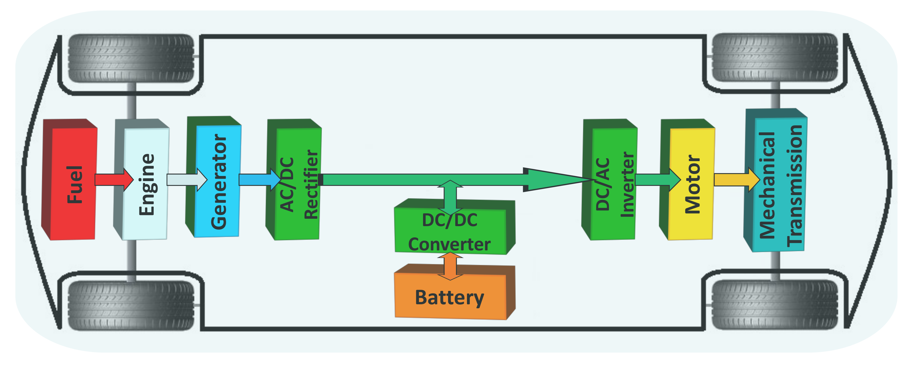
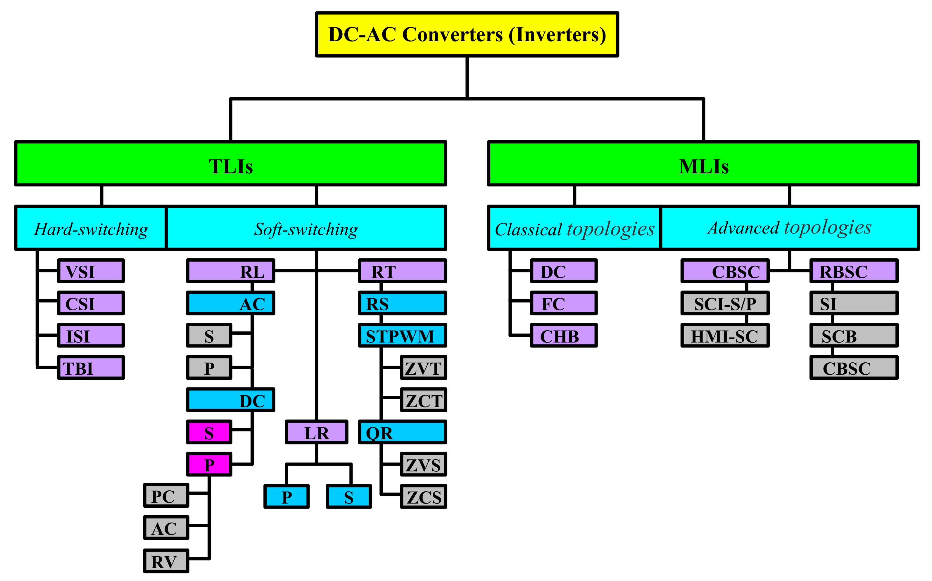
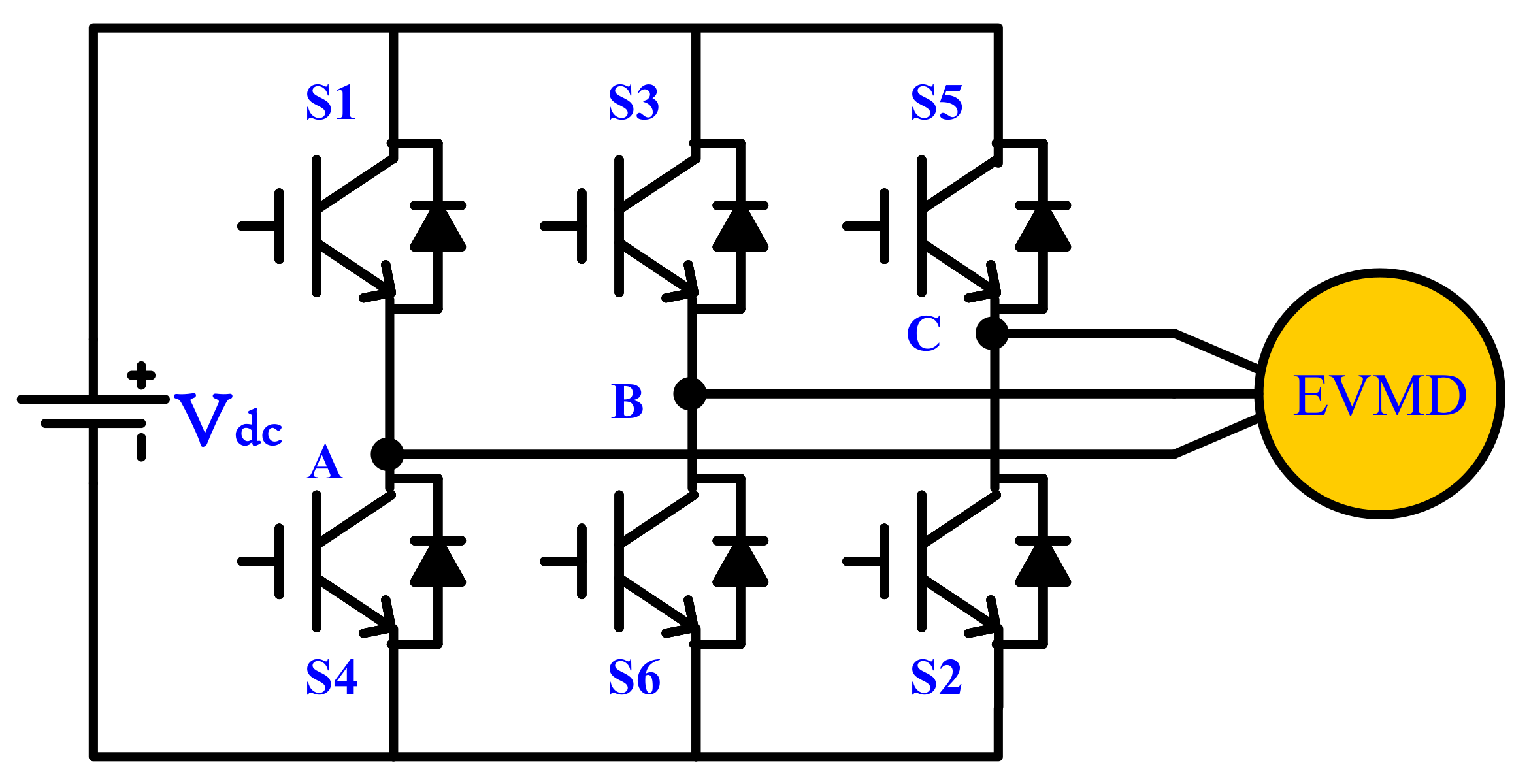
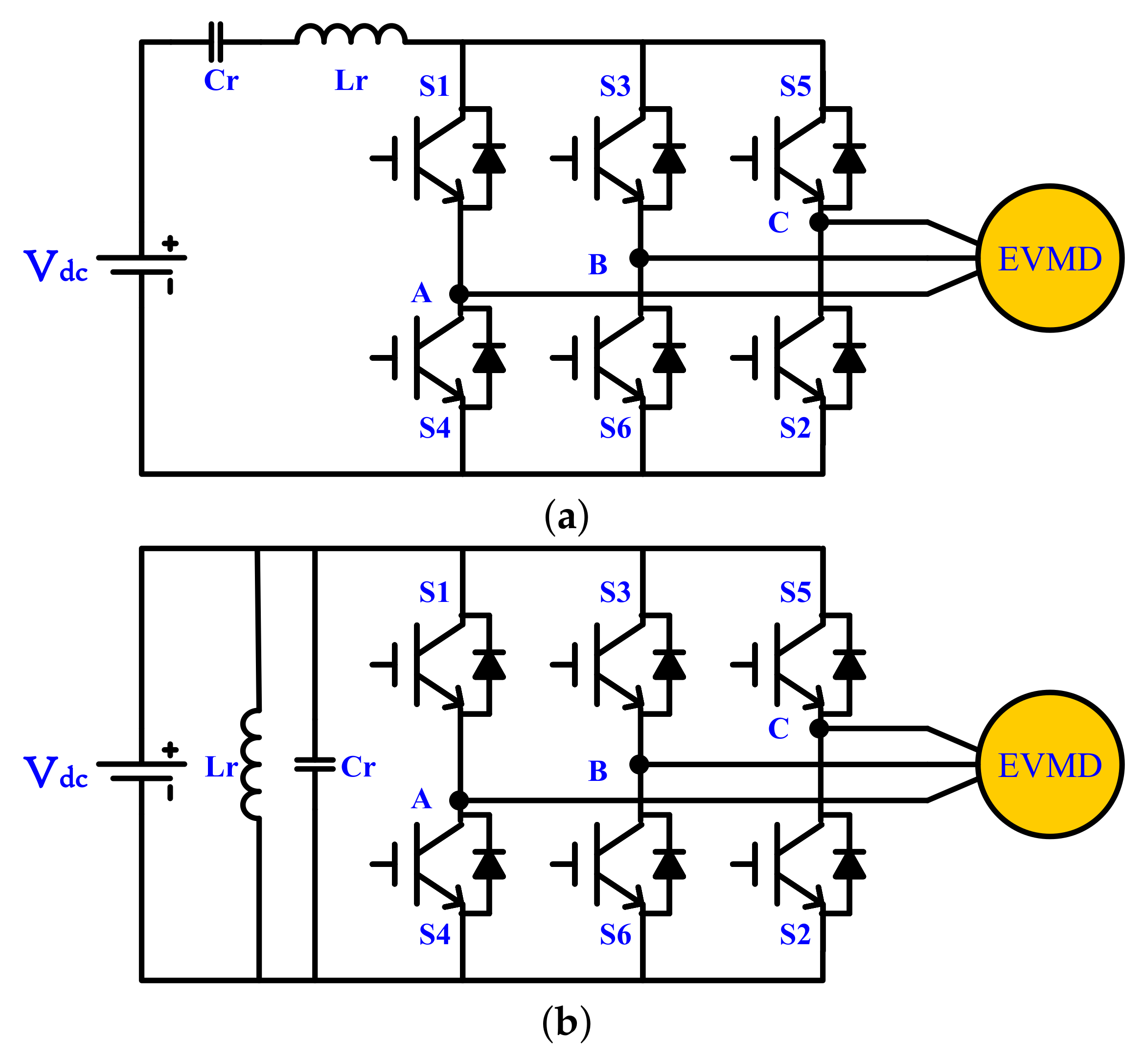
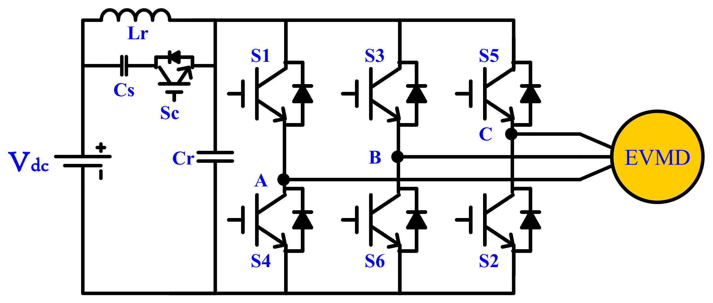
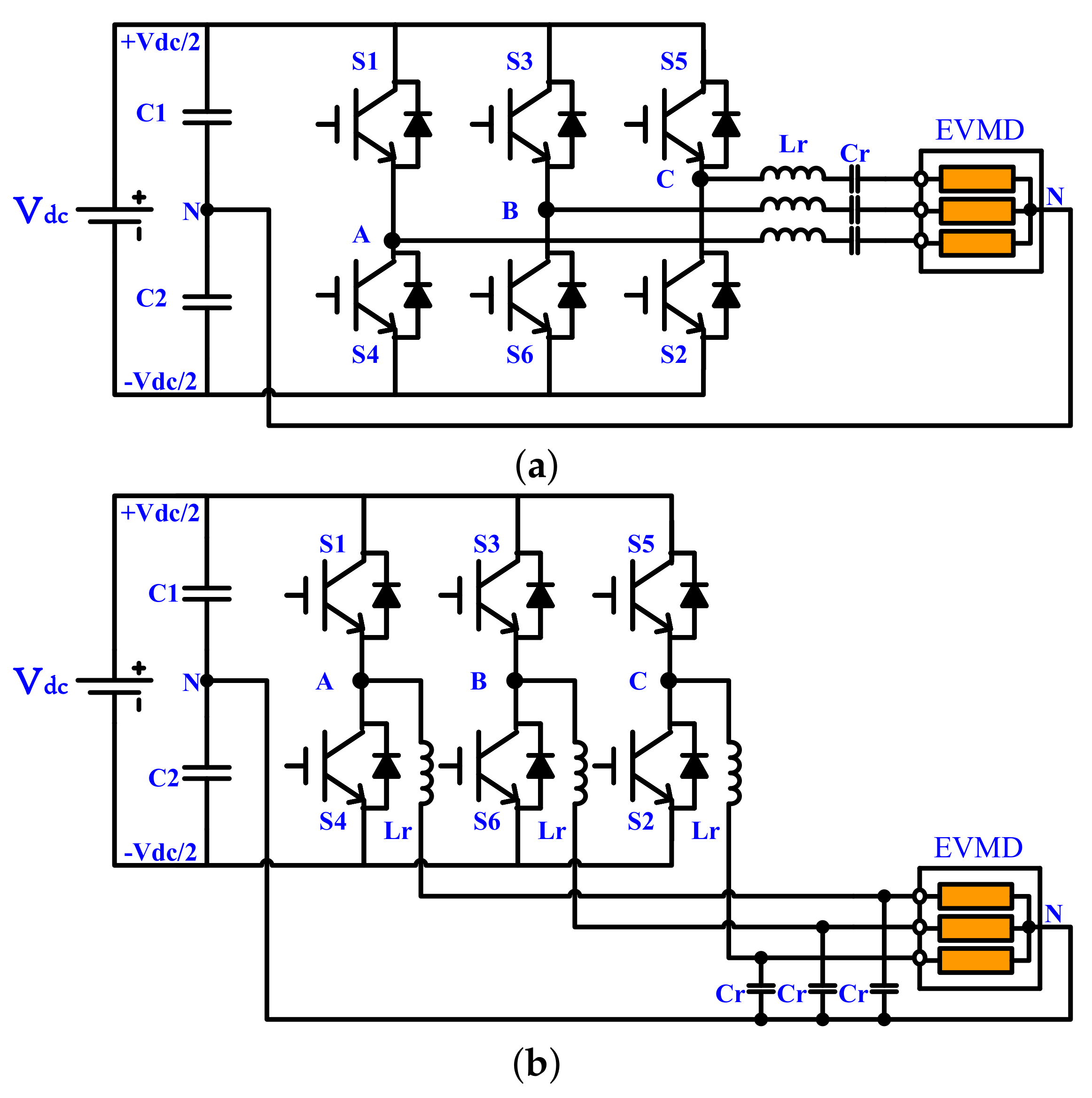
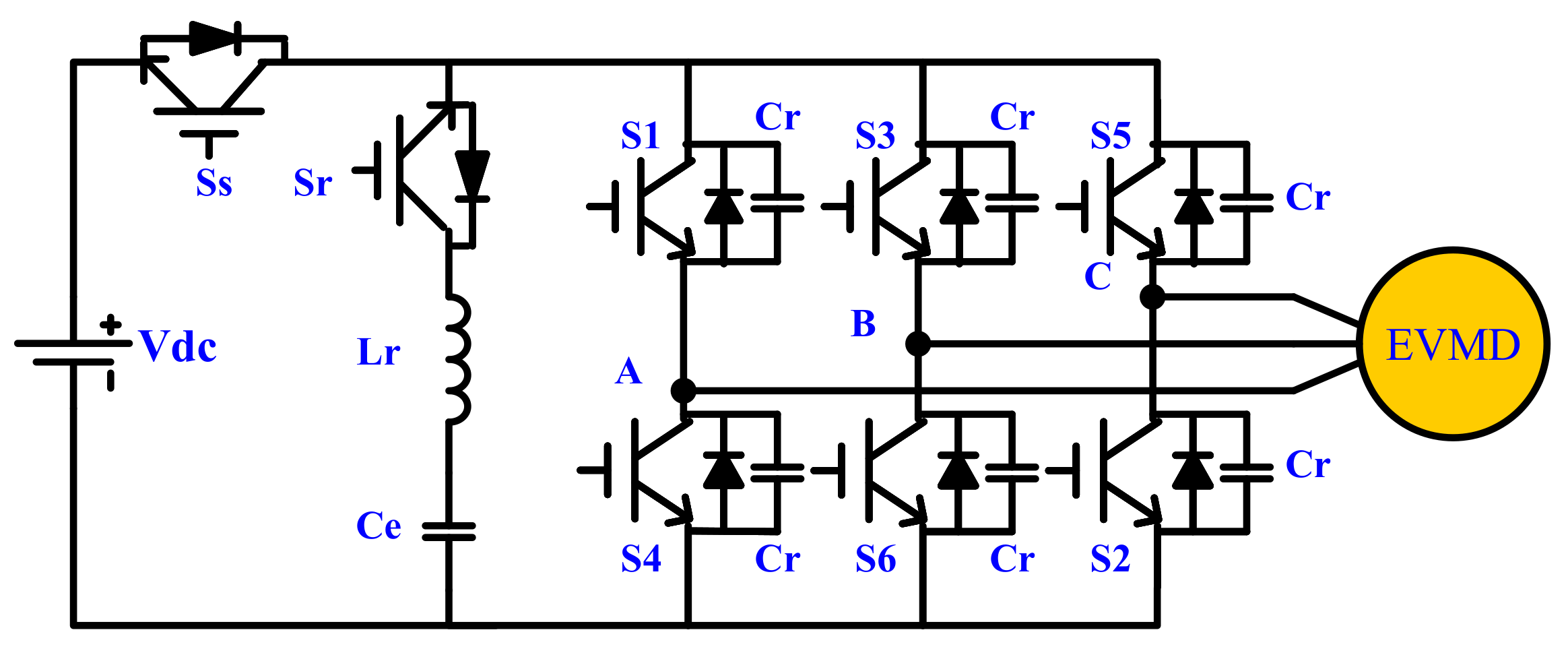
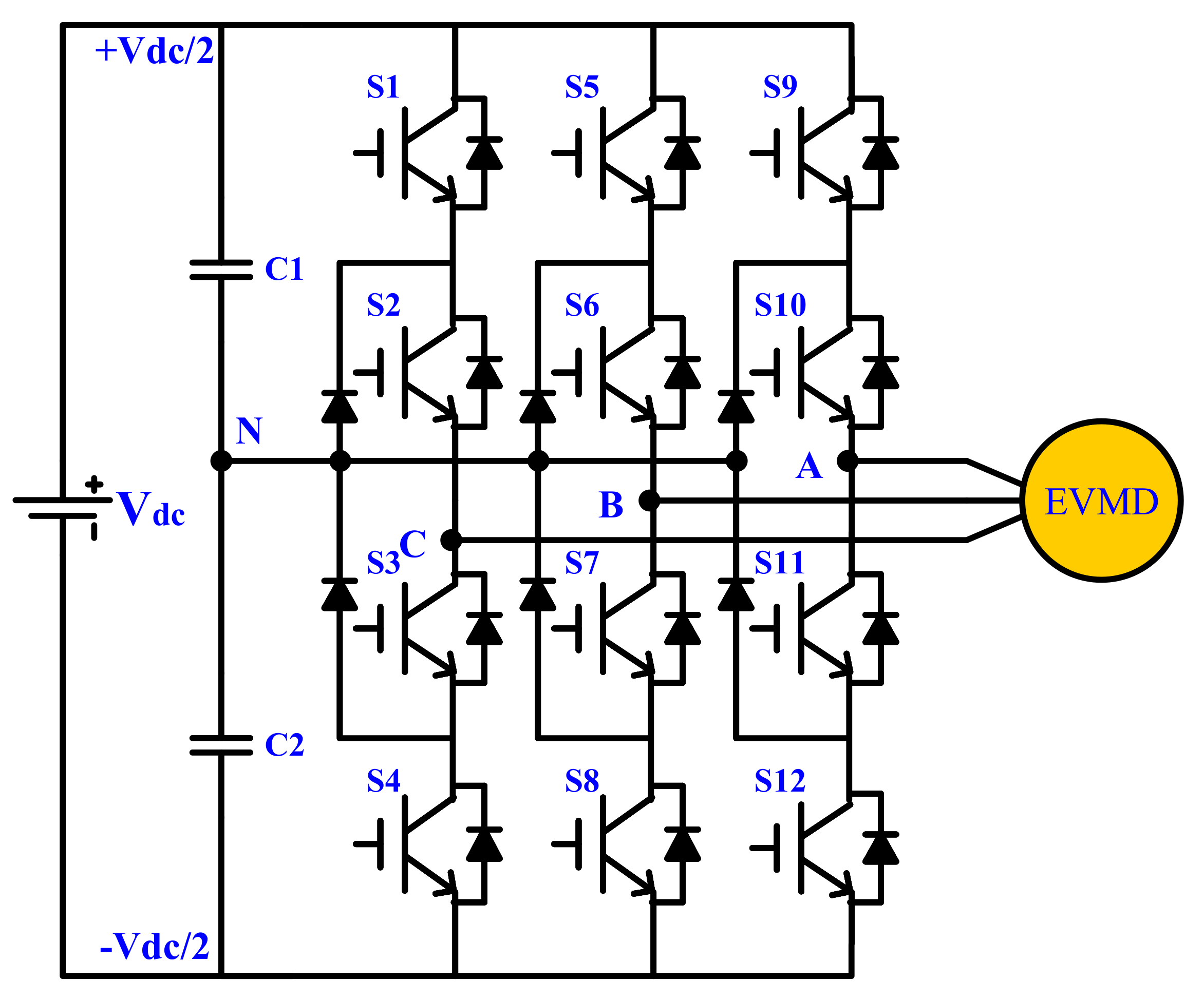
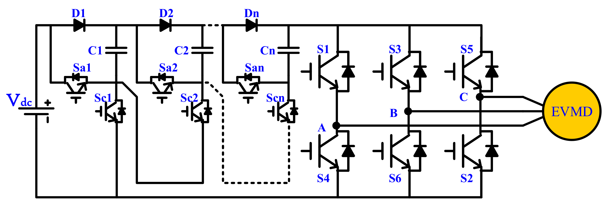
Table 1.
Summary of the Conventional Hard Switching Topologies and Applications.
| Inverter Type | Controller | Modulation Techniques & Control Strategies | Mode of Operation | Reference |
|---|---|---|---|---|
| VSI | PWM | Unipolar PWM | Buck | [1] |
| VSI | PWM | Pulse Width Modulation | Buck | [20] |
| VSI | PWM | high carrier frequency unipolar PWM modulation | Buck | [35] |
| VSI | SPWM | Sinusoidal pulse width modulation | Buck | [1,14,21] |
| CSI | PI | Dual Loop Control | Boost | [36] |
| CSI | SMC | Sliding Mode Control | Boost | [22] |
| CSI | SPWM | Sinusoidal pulse width modulation | Boost | [21,32,34] |
| CSI | PWM | Pulse width modulation | Buck, Boost and Buck-Boost | [37,38,39,40] |
| CSI | PWM | Boost the Voltage in Shoot Through the State | Modified as Improved SBI | [41] |
| CSI | PWM | Microcontroller-based reference-waveform generation Method | Boost | [42,43] |
| ISI | PWM | Modified PWM Space Vector Control | — | [44] |
| ISI | PWM | Shoot-through duty factor control and modulation index control | Modified multiple source application | [27] |
| ISI | PWM | Maximum Constant Boost with Third Harmonic Injection Control | — | [45] |
| ISI | PWM | Maximum Boost Control PWM Technique | — | [46] |
| TBI | SMC | Sliding Mode Control | Boost | [47,48,49,50,51] |
| TBI | PI | Dual Loop Control | Boost and Buck-Boost | [29,52,53,54,55,56,57,58] |
| TBI | PID | Ziegler-Nichols Tuning | Buck-Boost | [59,60] |
| TBI | PWM | Dual Loop Control | Boost | [61,62] |
| TBI | PWM | Unipolar PWM Control | Boost | [63] |
| TBI | PWM | One-Cycle Control | Boost | [64] |
| TBI | AFNNC | Adaptive Fuzzy Rule-Based Neural Network Control | Boost | [65,66] |
Table 2.
Comparison of various classical multilevel DC-AC inverters.
| Topology | Number of | ||||||
|---|---|---|---|---|---|---|---|
| DC Voltage Sources | Switches | Antiparallel Diodes | Close Diodes | Capacitors | Balancing Capacitors | Output Voltage Levels | |
| DC–MLI | 1 | 12 | 12 | 6 | 0 | 2 | 3 |
| FC–MLI | 1 | 12 | 12 | 0 | 3 | 2 | 3 |
| CHB–MLI | 3 | 12 | 12 | 0 | 0 | 0 | 3 |
Table 3.
Comparison of Several Advanced Multilevel DC-AC Inverter Topologies.
| Topology | Number of | ||||
|---|---|---|---|---|---|
| Voltage Levels in the Output | Active Switches | Diodes | Capacitors | Inductors | |
| CBSC | 13 | 10 | 12 | 6 | 1 |
| SCB | 13 | 11 | 3 | 2 | 1 |
| SCI-S/P | 13 | 15 | 15 | 6 | 0 |
| SI | 13 | 9 | 1 | 4 | 1 |
| HMI | 25 | 12 | 2 | 2 | 0 |
Publisher’s Note: MDPI stays neutral with regard to jurisdictional claims in published maps and institutional affiliations. |
© 2022 by the authors. Licensee MDPI, Basel, Switzerland. This article is an open access article distributed under the terms and conditions of the Creative Commons Attribution (CC BY) license (https://creativecommons.org/licenses/by/4.0/).
Share and Cite
MDPI and ACS Style
Sayed, K.; Almutairi, A.; Albagami, N.; Alrumayh, O.; Abo-Khalil, A.G.; Saleeb, H. A Review of DC-AC Converters for Electric Vehicle Applications. Energies 2022, 15, 1241. https://doi.org/10.3390/en15031241
AMA Style
Sayed K, Almutairi A, Albagami N, Alrumayh O, Abo-Khalil AG, Saleeb H. A Review of DC-AC Converters for Electric Vehicle Applications. Energies. 2022; 15(3):1241. https://doi.org/10.3390/en15031241
Chicago/Turabian StyleSayed, Khairy, Abdulaziz Almutairi, Naif Albagami, Omar Alrumayh, Ahmed G. Abo-Khalil, and Hedra Saleeb. 2022. "A Review of DC-AC Converters for Electric Vehicle Applications" Energies 15, no. 3: 1241. https://doi.org/10.3390/en15031241
Note that from the first issue of 2016, this journal uses article numbers instead of page numbers. See further details here.